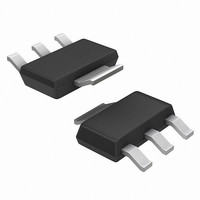
NTF5P03T3G ON Semiconductor, NTF5P03T3G Datasheet - Page 4

NTF5P03T3G
Manufacturer Part Number
NTF5P03T3G
Description
MOSFET P-CH 30V 3.7A SOT223
Manufacturer
ON Semiconductor
Datasheet
1.NTF5P03T3G.pdf
(7 pages)
Specifications of NTF5P03T3G
Fet Type
MOSFET P-Channel, Metal Oxide
Fet Feature
Logic Level Gate
Rds On (max) @ Id, Vgs
100 mOhm @ 5.2A, 10V
Drain To Source Voltage (vdss)
30V
Current - Continuous Drain (id) @ 25° C
3.7A
Vgs(th) (max) @ Id
3V @ 250µA
Gate Charge (qg) @ Vgs
38nC @ 10V
Input Capacitance (ciss) @ Vds
950pF @ 25V
Power - Max
1.56W
Mounting Type
Surface Mount
Package / Case
SOT-223 (3 leads + Tab), SC-73, TO-261
Configuration
Single Dual Drain
Transistor Polarity
P-Channel
Resistance Drain-source Rds (on)
0.1 Ohms
Forward Transconductance Gfs (max / Min)
3.9 S
Drain-source Breakdown Voltage
- 30 V
Gate-source Breakdown Voltage
+/- 20 V
Continuous Drain Current
- 5.2 A
Power Dissipation
3.13 W
Maximum Operating Temperature
+ 150 C
Mounting Style
SMD/SMT
Minimum Operating Temperature
- 55 C
Lead Free Status / RoHS Status
Lead free / RoHS Compliant
Other names
NTF5P03T3GOS
NTF5P03T3GOS
NTF5P03T3GOSTR
NTF5P03T3GOS
NTF5P03T3GOSTR
Available stocks
Company
Part Number
Manufacturer
Quantity
Price
Company:
Part Number:
NTF5P03T3G
Manufacturer:
ON
Quantity:
2 195
Company:
Part Number:
NTF5P03T3G
Manufacturer:
ON
Quantity:
30 000
Part Number:
NTF5P03T3G
Manufacturer:
ON/安森美
Quantity:
20 000
0.100
0.075
0.050
0.025
1.6
1.4
1.2
0.8
0.6
5
4
3
2
1
0
0
0
1
−50
T
0
V
V
J
V
GS
GS
= 25°C
V
V
GS
−V
−V
I
V
GS
GS
D
Figure 5. On−Resistance Variation with
= −10 V
GS
−25
= −8.0 V
DS,
Figure 1. On−Region Characteristics
= −2.0 A
= −6.0 V
GS,
0.3
= −4.5 V
= −4.3 V
= −10 V
Figure 3. On−Resistance versus
DRAIN−TO−SOURCE VOLTAGE (VOLTS)
GATE−TO−SOURCE VOLTAGE (VOLTS)
1
T
J
, JUNCTION TEMPERATURE (°C)
Gate−to−Source Voltage
0
0.6
Temperature
25
2
I
T
0.9
D
J
50
= −4.0 A
= 25°C
TYPICAL ELECTRICAL CHARACTERISTICS
3
75
1.2
V
V
V
V
V
V
100
V
GS
GS
GS
GS
GS
GS
GS
4
1.5
= −3.9 V
= −3.7 V
= −3.5 V
= −3.3 V
= −3.1 V
= −2.7 V
= −4.1 V
http://onsemi.com
125
NTF5P03T3
1.8
5
150
4
0.20
0.15
0.10
0.05
100
10
10
4
0
1
8
6
2
0
0
3
0
Figure 4. On−Resistance versus Drain Current
V
T
Figure 6. Drain−to−Source Leakage Current
T
V
J
GS
J
−V
DS
−V
T
= 25°C
= 100°C
1
J
= 0 V
DS,
3.5
GS,
≥ −10 V
= 25°C
Figure 2. Transfer Characteristics
10
DRAIN−TO−SOURCE VOLTAGE (VOLTS)
GATE−TO−SOURCE VOLTAGE (VOLTS)
−I
2
D,
DRAIN CURRENT (AMPS)
and Gate Voltage
4
T
versus Voltage
J
3
15
= −55°C
T
T
V
V
J
J
GS
GS
= 125°C
= 100°C
4.5
= −4.5 V
= −10 V
4
20
5
5
6
25
5.5
7
30
6
8


