NTJS3151PT1G ON Semiconductor, NTJS3151PT1G Datasheet

MOSFET P-CH 12V 2.7A SOT-363

NTJS3151PT1G

Manufacturer Part Number
NTJS3151PT1G
Description
MOSFET P-CH 12V 2.7A SOT-363
Manufacturer
ON Semiconductor
Datasheet

Specifications of NTJS3151PT1G

Fet Type
MOSFET P-Channel, Metal Oxide
Fet Feature
Logic Level Gate
Rds On (max) @ Id, Vgs
60 mOhm @ 3.3A, 4.5V
Drain To Source Voltage (vdss)
12V
Current - Continuous Drain (id) @ 25° C
2.7A
Vgs(th) (max) @ Id
400mV @ 100µA
Gate Charge (qg) @ Vgs
8.6nC @ 4.5V
Input Capacitance (ciss) @ Vds
850pF @ 12V
Power - Max
625mW
Mounting Type
Surface Mount
Package / Case
SC-70-6, SC-88, SOT-363
Configuration
Single Quad Drain
Transistor Polarity
N-Channel
Resistance Drain-source Rds (on)
0.06 Ohm @ 4.5 V
Forward Transconductance Gfs (max / Min)
15 S
Drain-source Breakdown Voltage
12 V
Gate-source Breakdown Voltage
+/- 12 V
Continuous Drain Current
2.7 A
Power Dissipation
625 mW
Maximum Operating Temperature
+ 150 C
Mounting Style
SMD/SMT
Minimum Operating Temperature
- 55 C
Lead Free Status / RoHS Status
Lead free / RoHS Compliant
Other names
NTJS3151PT1GOSTR

Available stocks

Company
Part Number
Manufacturer
Quantity
Price
Part Number:
NTJS3151PT1G
Manufacturer:
ON
Quantity:
5 385
Part Number:
NTJS3151PT1G
Manufacturer:
ON
Quantity:
30 000
Company:
Part Number:
NTJS3151PT1G
Quantity:
100
NTJS3151P
Trench Power MOSFET
12 V, 3.3 A, Single P−Channel,
ESD Protected SC−88
Features
Applications
Stresses exceeding Maximum Ratings may damage the device. Maximum
Ratings are stress ratings only. Functional operation above the Recommended
Operating Conditions is not implied. Extended exposure to stresses above the
Recommended Operating Conditions may affect device reliability.
1. Surface mounted on FR4 board using 1 in sq pad size
© Semiconductor Components Industries, LLC, 2006
March, 2006 − Rev. 2
MAXIMUM RATINGS
Continuous Drain
THERMAL RESISTANCE RATINGS
Drain−to−Source Voltage
Gate−to−Source Voltage
Power Dissipation
Pulsed Drain Current
Operating Junction and Storage Temperature
Source Current (Body Diode)
Lead Temperature for Soldering Purposes
Junction−to−Ambient – Steady State
Junction−to−Ambient − t ≤ 5 s
Junction−to−Lead – Steady State
Leading Trench Technology for Low R
SC−88 Small Outline (2x2 mm, SC70−6 Equivalent)
Gate Diodes for ESD Protection
Pb−Free Packages are Available
High Side Load Switch
Cell Phones, Computing, Digital Cameras, MP3s and PDAs
(Cu area = 1.127 in sq [1 oz] including traces).
Current (Note 1)
(Note 1)
(1/8” from case for 10 s)
Parameter
Parameter
(T
Steady
Steady
t ≤ 5 s
J
State
State
= 25°C unless otherwise stated)
T
T
T
T
t
A
A
A
A
p
= 10 ms
= 25 °C
= 85 °C
= 25 °C
= 25 °C
(Note 1)
DS(ON)
Symbol
Symbol
V
T
R
R
R
V
I
T
P
DSS
DM
STG
T
I
I
qJA
qJA
qJL
GS
D
S
J
D
L
Extending Battery Life
,
−55 to
Value
0.625
−2.7
−2.0
−3.3
−8.0
−0.8
Max
−12
±12
150
260
200
141
102
1
Units
Units
°C/W
°
°C
W
V
V
A
A
A
C
See detailed ordering and shipping information in the package
dimensions section on page 5 of this data sheet.
V
SC−88/SOT−363
(BR)DSS
−12 V
CASE 419B
(Note: Microdot may be in either location)
STYLE 28
G
G
D
D
ORDERING INFORMATION
TJ
M
G
1
133 mW @ −1.8 V
1
2
3
45 mW @ −4.5 V
67 mW @ −2.5 V
http://onsemi.com
SC−88 (SOT−363)
R
DS(on)
= Device Code
= Date Code
= Pb−Free Package
Top View
MARKING DIAGRAM &
3 kW
PIN ASSIGNMENT
Typ
Publication Order Number:
6
1
D
D
TJ M G
D
G
D
6
5
4
NTJS3151/D
G
S
D
S
I
−3.3 A
D
Max
D
D
S

Related parts for NTJS3151PT1G

NTJS3151PT1G Summary of contents

Page 1

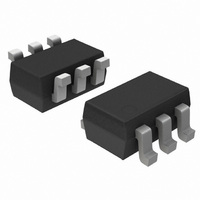
NTJS3151P Trench Power MOSFET 12 V, 3.3 A, Single P−Channel, ESD Protected SC−88 Features • Leading Trench Technology for Low R • SC−88 Small Outline (2x2 mm, SC70−6 Equivalent) • Gate Diodes for ESD Protection • Pb−Free Packages are Available ...

Page 2

ELECTRICAL CHARACTERISTICS Parameter OFF CHARACTERISTICS Drain−to−Source Breakdown Voltage Drain−to−Source Breakdown Voltage Temperature Coefficient Zero Gate Voltage Drain Current Gate−to−Source Leakage Current ON CHARACTERISTICS (Note 2) Gate Threshold Voltage Negative Threshold Temperature Coefficient Drain−to−Source On Resistance Forward Transconductance CHARGES AND CAPACITANCES ...

Page 3

TYPICAL PERFORMANCE CURVES −4 −3 −2 −V , DRAIN−TO−SOURCE VOLTAGE (VOLTS) DS Figure 1. On−Region Characteristics 0 −4 ...

Page 4

TYPICAL PERFORMANCE CURVES 1600 1400 1200 1000 800 600 400 200 C rss GATE−TO−SOURCE OR DRAIN−TO−SOURCE VOLTAGE (VOLTS) Figure 7. Capacitance Variation 10000 d(off 1000 t d(on) 100 1 10 ...

Page 5

... ORDERING INFORMATION Device NTJS3151PT1 NTJS3151PT1G NTJS3151PT2 NTJS3151PT2G †For information on tape and reel specifications, including part orientation and tape sizes, please refer to our Tape and Reel Packaging Specifications Brochure, BRD8011/D. Package SC−88 SC−88 (Pb−Free) SC−88 SC−88 (Pb−Free) http://onsemi.com 5 † Shipping 3000 Tape & Reel 3000 Tape & ...

Page 6

... Pb−Free strategy and soldering details, please download the ON Semiconductor Soldering and Mounting Techniques Reference Manual, SOLDERRM/D. ON Semiconductor and are registered trademarks of Semiconductor Components Industries, LLC (SCILLC). SCILLC reserves the right to make changes without further notice to any products herein ...

Related keywords