NTJS4160NT1G ON Semiconductor, NTJS4160NT1G Datasheet
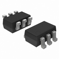
MOSFET N-CH 30V 1.8A SC88-6

NTJS4160NT1G

Manufacturer Part Number
NTJS4160NT1G
Description
MOSFET N-CH 30V 1.8A SC88-6
Manufacturer
ON Semiconductor
Datasheet

Specifications of NTJS4160NT1G

Fet Type
MOSFET N-Channel, Metal Oxide
Fet Feature
Logic Level Gate
Rds On (max) @ Id, Vgs
60 mOhm @ 2.6A, 10V
Drain To Source Voltage (vdss)
30V
Current - Continuous Drain (id) @ 25° C
1.8A
Vgs(th) (max) @ Id
2.4V @ 250µA
Gate Charge (qg) @ Vgs
2.75nC @ 4.5V
Input Capacitance (ciss) @ Vds
230pF @ 10V
Power - Max
300mW
Mounting Type
Surface Mount
Package / Case
SC-70-6, SC-88, SOT-363
Configuration
Single Quad Drain
Transistor Polarity
N-Channel
Resistance Drain-source Rds (on)
0.06 Ohm @ 10 V
Forward Transconductance Gfs (max / Min)
4.2 S
Drain-source Breakdown Voltage
30 V
Gate-source Breakdown Voltage
+/- 20 V
Continuous Drain Current
2.6 A
Power Dissipation
620 mW
Maximum Operating Temperature
+ 150 C
Mounting Style
SMD/SMT
Minimum Operating Temperature
- 55 C
Lead Free Status / RoHS Status
Lead free / RoHS Compliant
Other names
NTJS4160NT1G
NTJS4160NT1GOSTR

Available stocks

Company
Part Number
Manufacturer
Quantity
Price
Part Number:
NTJS4160NT1G
Manufacturer:
ON
Quantity:
30 000
Part Number:
NTJS4160NT1G
Manufacturer:
ON/安森美
Quantity:
20 000
Company:
Part Number:
NTJS4160NT1G
Quantity:
200
Company:
Part Number:
NTJS4160NT1G
Quantity:
200
NTJS4160N
Power MOSFET
30 V, 3.2 A, Single N-Channel, SC-88
Features
Applications
Stresses exceeding Maximum Ratings may damage the device. Maximum
Ratings are stress ratings only. Functional operation above the Recommended
Operating Conditions is not implied. Extended exposure to stresses above the
Recommended Operating Conditions may affect device reliability.
1. Surface mounted on FR4 board using 1 in sq pad size (Cu area = 1.127 in sq
2. Surface mounted on FR4 board using the minimum recommended pad size.
© Semiconductor Components Industries, LLC, 2008
March, 2008 - Rev. 1
MAXIMUM RATINGS
Continuous Drain
Current (Note 1)
Continuous Drain
Current (Note 2)
Drain-to-Source Voltage
Gate-to-Source Voltage
Power Dissipation
(Note 1)
Power Dissipation
(Note 2)
Pulsed Drain Current
Operating Junction and Storage Temperature
Source Current (Body Diode)
Lead Temperature for Soldering Purposes
(1/8” from case for 10 s)
Environments such as Portable Electronics
Cell Phones, PDAs, Media Players, etc.
Offers an Low R
Low Profile (< 1.1 mm) Allows it to fit Easily into Extremely Thin
Operates at Standard Logic Level Gate Drive
Low Gate Charge
This is a Pb-Free Device
DC-DC Converters (Buck and Boost Circuit)
Optimized for Battery Powered Portable Equipment such as,
Load Management
Battery Charging and OV IC Protection Circuits
[2 oz] including traces).
Parameter
DS(on)
(T
Steady
Steady
Steady
t ≤ 1 s
t ≤ 1 s
J
State
State
State
Solution in the SC-88 Package
= 25°C unless otherwise stated)
t
p
= 10 ms
T
T
T
T
T
T
T
A
A
A
A
A
A
A
= 25 °C
= 85 °C
= 25 °C
= 25 °C
= 25 °C
= 85 °C
= 25 °C
Symbol
V
T
V
I
T
P
P
DSS
DM
STG
T
I
I
I
GS
D
D
S
J
D
D
L
,
-55 to
Value
0.62
0.95
±20
150
260
2.6
1.9
3.2
1.8
1.3
0.3
1.3
30
10
1
Unit
°
°C
W
W
V
V
A
A
A
A
C
†For information on tape and reel specifications,
NTJS4160NT1G
V
including part orientation and tape sizes, please
refer to our Tape and Reel Packaging Specifications
Brochure, BRD8011/D.
SC-88 (SOT 363)
(BR)DSS
30 V
6
CASE 419B
Device
STYLE 28
G
D
D
T7
M
G
(Note: Microdot may be in either location)
ORDERING INFORMATION
1
1
2
3
http://onsemi.com
65 mW @ 4.5 V
45 mW @ 10 V
= Device Code
= Date Code
= Pb-Free Package
R
DS(on)
(SOT-363)
(Pb-Free)
Package
Top View
SC-88
SC-88
MARKING DIAGRAM
TYP
Publication Order Number:
1
T7 MG
3000 Units/Reel
G
6
5
4
Shipping
NTJS4160N/D
I
D
3.2 A
Max
D
D
S

Related parts for NTJS4160NT1G

NTJS4160NT1G Summary of contents

Page 1

... ° - 150 STG I 1 °C 260 T L Device NTJS4160NT1G †For information on tape and reel specifications, including part orientation and tape sizes, please refer to our Tape and Reel Packaging Specifications Brochure, BRD8011/D. 1 http://onsemi.com R TYP I Max DS(on 3 4.5 V MARKING DIAGRAM Device Code ...

Page 2

THERMAL RESISTANCE RATINGS Parameter Junction-to-Ambient – Steady State (Note 3) Junction-to-Ambient - t ≤ (Note 3) Junction-to-Ambient – Steady State (Note 4) 3. Surface mounted on FR4 board using pad size (Cu area = 1.127 ...

Page 3

TYPICAL PERFORMANCE CURVES 4 25° 0.5 1 1 DRAIN-TO-SOURCE VOLTAGE (VOLTS) DS Figure ...

Page 4

TYPICAL PERFORMANCE CURVES 400 350 300 250 C iss 200 150 100 C oss 50 C rss DRAIN-TO-SOURCE VOLTAGE (VOLTS) Figure 7. Capacitance Variation 100 ...

Page 5

... L 0.40 0.0157 *For additional information on our Pb-Free strategy and soldering details, please download the ON Semiconductor Soldering and Mounting Techniques Reference Manual, SOLDERRM/D. N. American Technical Support: 800-282-9855 Toll Free  USA/Canada Europe, Middle East and Africa Technical Support:  Phone: 421 33 790 2910 Japan Customer Focus Center   ...

Related keywords