STW20NM50FD STMicroelectronics, STW20NM50FD Datasheet - Page 2
STW20NM50FD
Manufacturer Part Number
STW20NM50FD
Description
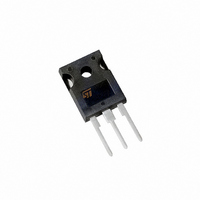
MOSFET N-CH 500V 20A TO-247
Manufacturer
STMicroelectronics
Series
FDmesh™r
Datasheet
1.STW20NM50FD.pdf
(8 pages)
Specifications of STW20NM50FD
Fet Type
MOSFET N-Channel, Metal Oxide
Fet Feature
Standard
Rds On (max) @ Id, Vgs
250 mOhm @ 10A, 10V
Drain To Source Voltage (vdss)
500V
Current - Continuous Drain (id) @ 25° C
20A
Vgs(th) (max) @ Id
5V @ 250µA
Gate Charge (qg) @ Vgs
53nC @ 10V
Input Capacitance (ciss) @ Vds
1380pF @ 25V
Power - Max
214W
Mounting Type
Through Hole
Package / Case
TO-247-3
Configuration
Single
Transistor Polarity
N-Channel
Resistance Drain-source Rds (on)
0.25 Ohm @ 10 V
Drain-source Breakdown Voltage
500 V
Gate-source Breakdown Voltage
+/- 30 V
Continuous Drain Current
20 A
Power Dissipation
214000 mW
Maximum Operating Temperature
+ 150 C
Mounting Style
Through Hole
Minimum Operating Temperature
- 65 C
Lead Free Status / RoHS Status
Lead free / RoHS Compliant
Other names
497-2717-5
Available stocks
Company
Part Number
Manufacturer
Quantity
Price
Company:

Part Number:
STW20NM50FD
Manufacturer:
ST
Quantity:
4 300
Part Number:
STW20NM50FD
Manufacturer:
ST
Quantity:
20 000


STW20NM50FD
THERMAL DATA
AVALANCHE CHARACTERISTICS
ELECTRICAL CHARACTERISTICS (TCASE = 25 °C UNLESS OTHERWISE SPECIFIED)
OFF
ON (1)
DYNAMIC
2/8
C
Rthj-case
Rthj-amb
V
Symbol
Symbol
Symbol
Symbol
R
oss eq.
V
(BR)DSS
g
I
I
C
DS(on)
C
E
GS(th)
C
fs
I
GSS
1. Pulsed: Pulse duration = 300 µs, duty cycle 1.5 %.
2. C
DSS
R
AR
T
oss
AS
rss
iss
(1)
g
l
V
DSS
oss eq.
(2)
.
is defined as a constant equivalent capacitance giving the same charging time as C
Avalanche Current, Repetitive or Not-Repetitive
(pulse width limited by T
Single Pulse Avalanche Energy
(starting T
Drain-source
Breakdown Voltage
Zero Gate Voltage
Drain Current (V
Gate-body Leakage
Current (V
Gate Threshold Voltage
Static Drain-source On
Resistance
Forward Transconductance
Input Capacitance
Output Capacitance
Reverse Transfer
Capacitance
Equivalent Output
Capacitance
Gate Input Resistance
Thermal Resistance Junction-case
Thermal Resistance Junction-ambient
Maximum Lead Temperature For Soldering Purpose
Parameter
Parameter
Parameter
j
DS
= 25 °C, I
= 0)
GS
= 0)
D
= I
j
max)
AR
Parameter
, V
DD
I
V
V
V
V
V
V
I
V
f=1 MHz Gate DC Bias=0
Test Signal Level=20mV
Open Drain
D
D
V
= 35 V)
DS
DS
GS
DS
GS
DS
GS
DS
= 250 µA, V
= 10A
= Max Rating
= Max Rating, T
= V
> I
= ±30V
= 10V, I
= 0V, V
= 25V, f = 1 MHz, V
D(on)
Test Conditions
Test Conditions
Test Conditions
GS
, I
DS
D
x R
D
= 10A
GS
= 250µA
= 0V to 400V
DS(on)max,
Max
Max
= 0
C
= 125 °C
GS
= 0
Min.
Min.
Min.
500
3
oss
0.585
300
30
when V
Max Value
1380
700
Typ.
Typ.
0.22
Typ.
290
130
2.8
10
40
4
9
DS
increases from 0 to 80%
Max.
±100
Max.
Max.
0.25
10
1
5
°C/W
°C/W
Unit
Unit
Unit
Unit
mJ
µA
µA
°C
nA
pF
pF
pF
pF
A
V
V
S
Related parts for STW20NM50FD
Image
Part Number
Description
Manufacturer
Datasheet
Request
R


Part Number:
Description:
STMicroelectronics [RIPPLE-CARRY BINARY COUNTER/DIVIDERS]
Manufacturer:
STMicroelectronics
Datasheet:
Part Number:
Description:
STMicroelectronics [LIQUID-CRYSTAL DISPLAY DRIVERS]
Manufacturer:
STMicroelectronics
Datasheet:

Part Number:
Description:
BOARD EVAL FOR MEMS SENSORS
Manufacturer:
STMicroelectronics
Datasheet:
Part Number:
Description:
NPN TRANSISTOR POWER MODULE
Manufacturer:
STMicroelectronics
Datasheet:
Part Number:
Description:
TURBOSWITCH ULTRA-FAST HIGH VOLTAGE DIODE
Manufacturer:
STMicroelectronics
Datasheet:
Part Number:
Description:
Manufacturer:
STMicroelectronics
Datasheet:
Part Number:
Description:
DIODE / SCR MODULE
Manufacturer:
STMicroelectronics
Datasheet:
Part Number:
Description:
DIODE / SCR MODULE
Manufacturer:
STMicroelectronics
Datasheet:
Part Number:
Description:
Search -----> STE16N100
Manufacturer:
STMicroelectronics
Datasheet:
Part Number:
Description:
Search ---> STE53NA50
Manufacturer:
STMicroelectronics
Datasheet:
Part Number:
Description:
NPN Transistor Power Module
Manufacturer:
STMicroelectronics
Datasheet: