STW21NM50N STMicroelectronics, STW21NM50N Datasheet
STW21NM50N
Specifications of STW21NM50N
Available stocks


Related parts for STW21NM50N


STW21NM50N Summary of contents
Page 1
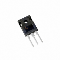
N-channel 500 V, 0.11 Ω MDmesh™ II Power MOSFET Features V DSS Type (@Tjmax) STB25NM50N 550 V STB25NM50N-1 550 V STF25NM50N 550 V STP25NM50N 550 V STW25NM50N 550 V 1. Limited only by maximum temperature allowed ■ 100% ...
Page 2
Contents Contents 1 Electrical ratings . . . . . . . . . . . . . . . . . . . . . . . . . . . . . . . . . . . ...
Page 3
STx25NM50N 1 Electrical ratings Table 2. Absolute maximum ratings Symbol V Drain-source voltage ( Gate- source voltage GS I Drain current (continuous Drain current (continuous (2) I Drain current (pulsed) DM ...
Page 4
Electrical characteristics 2 Electrical characteristics (T =25°C unless otherwise specified) CASE Table 5. On/off states Symbol Drain-source V (BR)DSS breakdown voltage (1) dv/dt Drain source voltage slope Zero gate voltage I DSS drain current (V Gate-body leakage I GSS current ...
Page 5
STx25NM50N Table 7. Switching times Symbol t Turn-on delay time d(on) t Rise time r t Turn-off delay time d(off) t Fall time f Table 8. Source drain diode Symbol I Source-drain current SD (1) I Source-drain current (pulsed) SDM ...
Page 6
Electrical characteristics 2.1 Electrical characteristics (curves) Figure 2. Safe operating area for TO-220 / D²PAK / I²PAK Figure 4. Safe operating area for TO-220FP Figure 6. Safe operating area for TO-247 6/18 Figure 3. Thermal impedance for TO-220 / D²PAK ...
Page 7
STx25NM50N Figure 8. Output characteristics Figure 10. Transconductance Figure 12. Gate charge vs gate-source voltage Figure 13. Capacitance variations Electrical characteristics Figure 9. Transfer characteristics Figure 11. Static drain-source on resistance 7/18 ...
Page 8
Electrical characteristics Figure 14. Normalized gate threshold voltage vs temperature Figure 16. Source-drain diode forward characteristics 8/18 Figure 15. Normalized on resistance vs temperature Figure 17. Normalized B VDSS STx25NM50N vs temperature ...
Page 9
STx25NM50N 3 Test circuit Figure 18. Switching times test circuit for resistive load Figure 20. Test circuit for inductive load switching and diode recovery times Figure 22. Unclamped inductive waveform Figure 19. Gate charge test circuit Figure 21. Unclamped Inductive ...
Page 10
Package mechanical data 4 Package mechanical data In order to meet environmental requirements, ST offers these devices in ECOPACK® packages. These packages have a Lead-free second level interconnect. The category of second level interconnect is marked on the package and ...
Page 11
STx25NM50N Dim L20 L30 ∅P Q TO-220 mechanical data mm Min Typ Max 4.40 4.60 0.61 0.88 1.14 1.70 0.48 0.70 15.25 15.75 1.27 10 10.40 ...
Page 12
Package mechanical data Dim 12/18 D²PAK (TO-263) mechanical data mm Min Typ Max 4.40 4.60 0.03 0.23 0.70 0.93 1.14 1.70 ...
Page 13
STx25NM50N Dim I²PAK (TO-262) mechanical data mm Min Typ Max 4.40 4.60 2.40 2.72 0.61 0.88 1.14 1.70 0.49 0.70 1.23 1.32 8.95 9.35 2.40 2.70 4.95 ...
Page 14
Package mechanical data DIM Ø 14/18 TO-220FP MECHANICAL DATA mm. MIN. TYP MAX. 4.4 4.6 2.5 2.7 2.5 2.75 0.45 0.7 0.75 1 1.15 ...
Page 15
STx25NM50N Dim øP øR S TO-247 Mechanical data mm. Min. Typ 4.85 2.20 1.0 2.0 3.0 0.40 19.85 15.45 5.45 14.20 3.70 18.50 3.55 4.50 5.50 Package mechanical ...
Page 16
Packaging mechanical data 5 Packaging mechanical data 2 D PAK FOOTPRINT TAPE MECHANICAL DATA mm DIM. MIN. MAX. A0 10.5 10.7 B0 15.7 15.9 D 1.5 1.6 D1 1.59 1.61 E 1.65 1.85 F 11.4 11.6 K0 4.8 5.0 P0 ...
Page 17
STx25NM50N 6 Revision history Table 9. Document revision history Date 30-Nov-2004 08-Mar-2005 22-Mar-2005 13-Apr-2005 28-Apr-2005 16-May-2005 17-Jun-2005 07-Sep-2005 05-Oct-2005 09-Nov-2005 14-Nov-2006 19-Jan-2007 17-Nov-2008 Revision 1 First release. 2 Inserted curves 3 Modified title 4 Modified some values 5 Modified some ...
Page 18
... Information in this document is provided solely in connection with ST products. STMicroelectronics NV and its subsidiaries (“ST”) reserve the right to make changes, corrections, modifications or improvements, to this document, and the products and services described herein at any time, without notice. All ST products are sold pursuant to ST’s terms and conditions of sale. ...