IRFP2907ZPBF International Rectifier, IRFP2907ZPBF Datasheet - Page 2
IRFP2907ZPBF
Manufacturer Part Number
IRFP2907ZPBF
Description
MOSFET N-CH 75V 90A TO-247AC
Manufacturer
International Rectifier
Series
HEXFET®r
Specifications of IRFP2907ZPBF
Fet Type
MOSFET N-Channel, Metal Oxide
Fet Feature
Standard
Rds On (max) @ Id, Vgs
4.5 mOhm @ 90A, 10V
Drain To Source Voltage (vdss)
75V
Current - Continuous Drain (id) @ 25° C
90A
Vgs(th) (max) @ Id
4V @ 250µA
Gate Charge (qg) @ Vgs
270nC @ 10V
Input Capacitance (ciss) @ Vds
7500pF @ 25V
Power - Max
310W
Mounting Type
Through Hole
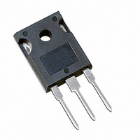
Package / Case
TO-247-3 (Straight Leads), TO-247AC
Current, Drain
170 A
Gate Charge, Total
180 nC
Package Type
TO-247AC
Polarization
N-Channel
Power Dissipation
310 W
Resistance, Drain To Source On
4.5 Milliohms
Temperature, Operating, Maximum
+175 °C
Temperature, Operating, Minimum
-55 °C
Time, Turn-off Delay
97 ns
Time, Turn-on Delay
19 ns
Transconductance, Forward
180 S
Voltage, Breakdown, Drain To Source
75 V
Voltage, Forward, Diode
1.3 V
Voltage, Gate To Source
±20 V
Transistor Polarity
N-Channel
Drain-source Breakdown Voltage
75 V
Gate-source Breakdown Voltage
20 V
Continuous Drain Current
170 A
Mounting Style
Through Hole
Gate Charge Qg
180 nC
Lead Free Status / RoHS Status
Lead free / RoHS Compliant
Other names
*IRFP2907ZPBF
Available stocks
Company
Part Number
Manufacturer
Quantity
Price
Company:

Part Number:
IRFP2907ZPBF
Manufacturer:
VISHAY
Quantity:
10 000


‚
ƒ
„
V
∆ΒV
R
V
gfs
I
I
Q
Q
Q
t
t
t
t
L
L
C
C
C
C
C
C
I
I
V
t
Q
t
Static @ T
Diode Characteristics
DSS
GSS
d(on)
r
d(off)
f
S
SM
rr
on
D
S
(BR)DSS
DS(on)
GS(th)
iss
oss
rss
oss
oss
oss
SD
2
g
gs
gd
rr
Repetitive rating; pulse width limited by
L=0.13mH, R
Part not recommended for use above this value.
I
Pulse width ≤ 1.0ms; duty cycle ≤ 2%.
T
max. junction temperature. (See fig. 11).
Limited by T
SD
J
DSS
eff.
≤ 175°C.
≤ 90A, di/dt ≤ 340A/µs, V
/∆T
J
J
Jmax
G
Drain-to-Source Breakdown Voltage
Breakdown Voltage Temp. Coefficient
Static Drain-to-Source On-Resistance
Gate Threshold Voltage
Forward Transconductance
Drain-to-Source Leakage Current
Gate-to-Source Forward Leakage
Gate-to-Source Reverse Leakage
Total Gate Charge
Gate-to-Source Charge
Gate-to-Drain ("Miller") Charge
Turn-On Delay Time
Rise Time
Turn-Off Delay Time
Fall Time
Internal Drain Inductance
Internal Source Inductance
Input Capacitance
Output Capacitance
Reverse Transfer Capacitance
Output Capacitance
Output Capacitance
Effective Output Capacitance
Continuous Source Current
(Body Diode)
Pulsed Source Current
(Body Diode)
Diode Forward Voltage
Reverse Recovery Time
Reverse Recovery Charge
Forward Turn-On Time
= 25°C (unless otherwise specified)
= 25Ω, I
, starting T
Parameter
AS
= 90A, V
Parameter
J
DD
™
= 25°C,
≤ V
GS
(BR)DSS
=10V.
,
Intrinsic turn-on time is negligible (turn-on is dominated by LS+LD)
Min. Typ. Max. Units
Min. Typ. Max. Units
…
†
‡
ˆ
–––
–––
–––
180
–––
–––
–––
–––
–––
–––
–––
–––
–––
–––
–––
–––
–––
–––
–––
–––
–––
–––
–––
–––
–––
–––
–––
2.0
75
C
charging time as C
Limited by T
This value determined from sample failure population. 100%
tested to this value in production.
R
avalanche performance.
oss
θ
is measured at
0.069
7500
3640
1020
–––
–––
–––
–––
–––
–––
–––
180
140
100
970
510
650
–––
–––
–––
eff. is a fixed capacitance that gives the same
3.5
5.0
46
65
19
97
13
41
59
-200
–––
–––
–––
–––
–––
–––
250
200
270
–––
–––
–––
–––
–––
–––
–––
–––
–––
–––
–––
680
Jmax
4.5
4.0
1.3
20
90
61
89
, see Fig.12a, 12b, 15, 16 for typical repetitive
oss
V/°C
mΩ
µA
nA
nC
nH
nC
ns
pF
ns
V
V
S
A
V
J
while V
V
Reference to 25°C, I
V
V
V
V
V
V
V
I
V
V
V
I
R
V
Between lead,
6mm (0.25in.)
from package
and center of die contact
V
V
ƒ = 1.0MHz, See Fig. 5
V
V
V
MOSFET symbol
showing the
integral reverse
p-n junction diode.
T
T
di/dt = 100A/µs
D
D
J
J
GS
GS
DS
DS
DS
DS
GS
GS
DS
GS
DD
GS
GS
DS
GS
GS
GS
G
= 90A
= 90A
= 25°C, I
= 25°C, I
DS
= 2.5Ω
= V
= 25V, I
= 75V, V
= 75V, V
= 60V
= 25V
= 0V, I
= 10V, I
= 20V
= -20V
= 10V
= 38V
= 10V
= 0V
= 0V, V
= 0V, V
= 0V, V
is rising from 0 to 80% V
GS
, I
f
f
Conditions
D
Conditions
D
DS
S
F
D
D
DS
DS
= 250µA
GS
GS
= 250µA
= 90A, V
= 90A
= 90A, V
= 90A
= 0V to 60V
= 1.0V, ƒ = 1.0MHz
= 60V, ƒ = 1.0MHz
f
= 0V
= 0V, T
D
f
= 1mA
GS
DD
J
G
= 125°C
= 38V
= 0V
G
DSS
f
S
D
S
D
.
Related parts for IRFP2907ZPBF
Image
Part Number
Description
Manufacturer
Datasheet
Request
R

Part Number:
Description:
Manufacturer:
International Rectifier Corp.
Datasheet:
Part Number:
Description:
SCHOTTKY RECTIFIER
Manufacturer:
International Rectifier Corp.
Datasheet:
Part Number:
Description:
SCHOTTKY RECTIFIER
Manufacturer:
International Rectifier Corp.
Datasheet:
Part Number:
Description:
SCHOTTKY RECTIFIER
Manufacturer:
International Rectifier Corp.
Datasheet:
Part Number:
Description:
SCHOTTKY RECTIFIER
Manufacturer:
International Rectifier Corp.
Datasheet:
Part Number:
Description:
SCHOTTKY RECTIFIER
Manufacturer:
International Rectifier Corp.
Datasheet:
Part Number:
Description:
SCHOTTKY RECTIFIER
Manufacturer:
International Rectifier Corp.
Datasheet:
Part Number:
Description:
SCHOTTKY RECTIFIER
Manufacturer:
International Rectifier Corp.
Datasheet:
Part Number:
Description:
SCHOTTKY RECTIFIER
Manufacturer:
International Rectifier Corp.
Datasheet:
Part Number:
Description:
SCHOTTKY RECTIFIER
Manufacturer:
International Rectifier Corp.
Datasheet:
Part Number:
Description:
SCHOTTKY RECTIFIER
Manufacturer:
International Rectifier Corp.
Datasheet:
Part Number:
Description:
SCHOTTKY RECTIFIER
Manufacturer:
International Rectifier Corp.
Datasheet:
Part Number:
Description:
SCHOTTKY RECTIFIER
Manufacturer:
International Rectifier Corp.
Datasheet:
Part Number:
Description:
SCHOTTKY RECTIFIER
Manufacturer:
International Rectifier Corp.
Datasheet:
Part Number:
Description:
SCHOTTKY RECTIFIER
Manufacturer:
International Rectifier Corp.
Datasheet: