STP5NK100Z STMicroelectronics, STP5NK100Z Datasheet - Page 2
STP5NK100Z
Manufacturer Part Number
STP5NK100Z
Description
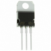
MOSFET N-CH 1KV 3.5A TO-220
Manufacturer
STMicroelectronics
Series
SuperMESH™r
Specifications of STP5NK100Z
Fet Type
MOSFET N-Channel, Metal Oxide
Fet Feature
Standard
Rds On (max) @ Id, Vgs
3.7 Ohm @ 1.75A, 10V
Drain To Source Voltage (vdss)
1000V (1kV)
Current - Continuous Drain (id) @ 25° C
3.5A
Vgs(th) (max) @ Id
4.5V @ 100µA
Gate Charge (qg) @ Vgs
59nC @ 10V
Input Capacitance (ciss) @ Vds
1154pF @ 25V
Power - Max
125W
Mounting Type
Through Hole
Package / Case
TO-220-3 (Straight Leads)
Configuration
Single
Transistor Polarity
N-Channel
Resistance Drain-source Rds (on)
3.7 Ohm @ 10 V
Forward Transconductance Gfs (max / Min)
4 S
Drain-source Breakdown Voltage
1000 V
Gate-source Breakdown Voltage
+/- 30 V
Continuous Drain Current
3.5 A
Power Dissipation
125000 mW
Maximum Operating Temperature
+ 150 C
Mounting Style
Through Hole
Minimum Operating Temperature
- 55 C
Continuous Drain Current Id
3.5A
Drain Source Voltage Vds
1kV
On Resistance Rds(on)
3.7ohm
Rds(on) Test Voltage Vgs
10V
Threshold Voltage Vgs Typ
3.75V
Rohs Compliant
Yes
Lead Free Status / RoHS Status
Lead free / RoHS Compliant
Other names
497-4382-5
Available stocks
Company
Part Number
Manufacturer
Quantity
Price
Company:

Part Number:
STP5NK100Z
Manufacturer:
ST
Quantity:
20 000
Company:
Part Number:
STP5NK100Z
Manufacturer:
STMicroelectronics
Quantity:
180
Part Number:
STP5NK100Z
Manufacturer:
ST
Quantity:
20 000


STP5NK100Z - STF5NK100Z - STW5NK100Z
Table 3: Absolute Maximum ratings
( ) Pulse width limited by safe operating area
(1) I
(*) Limited only by maximum temperature allowed
Table 4: Thermal Data
Table 5: Avalanche Characteristics
Table 6: Gate-Source Zener Diode
PROTECTION FEATURES OF GATE-TO-SOURCE ZENER DIODES
The built-in back-to-back Zener diodes have specifically been designed to enhance not only the device’s
ESD capability, but also to make them safely absorb possible voltage transients that may occasionally be
applied from gate to source. In this respect the Zener voltage is appropriate to achieve an efficient and
cost-effective intervention to protect the device’s integrity. These integrated Zener diodes thus avoid the
usage of external components.
2/12
V
Rthj-case
Rthj-amb
Symbol
Symbol
Symbol
dv/dt (1)
SD
BV
ESD(G-S)
I
V
DM
P
V
V
V
E
T
I
DGR
TOT
I
I
AR
ISO
T
T
stg
GSO
DS
GS
AS
D
D
3.5A, di/dt 200A/µs, V
j
l
( )
Avalanche Current, Repetitive or Not-Repetitive
(pulse width limited by T
Single Pulse Avalanche Energy
(starting T
Gate-Source Breakdown
Voltage
Thermal Resistance Junction-case Max
Thermal Resistance Junction-ambient Max
Maximum Lead Temperature For Soldering Purpose
Drain-source Voltage (V
Drain-gate Voltage (R
Gate- source Voltage
Drain Current (continuous) at T
Drain Current (continuous) at T
Drain Current (pulsed)
Total Dissipation at T
Derating Factor
Gate source ESD(HBM-C=100pF, R=1.5K
Peak Diode Recovery voltage slope
Insulation Withstand Voltage (DC)
Operating Junction Temperature
Storage Temperature
Parameter
j
= 25 °C, I
DD
V
(BR)DSS
Parameter
Parameter
D
C
GS
= I
= 25°C
, T
GS
j
= 20 k )
max)
AR
j
Igs=± 1mA (Open Drain)
= 0)
, V
T
JMAX.
DD
Test Conditions
C
C
= 25°C
= 100°C
= 50 V)
STW5NK100Z
STP5NK100Z
Min.
30
TO-220
TO-247
125
3.5
2.2
14
1
-
1
Max Value
-55 to 150
-55 to 150
Value
Typ.
1000
1000
4000
62.5
± 30
300
250
3.5
4.5
STF5NK100Z
TO-220FP
3.5 (*)
2.2 (*)
14 (*)
2500
0.24
4.2
30
Max.
°C/W
°C/W
Unit
Unit
W/°C
Unit
V/ns
mJ
°C
°C
°C
A
V
W
V
V
V
A
A
A
V
V
Related parts for STP5NK100Z
Image
Part Number
Description
Manufacturer
Datasheet
Request
R

Part Number:
Description:
STMicroelectronics [RIPPLE-CARRY BINARY COUNTER/DIVIDERS]
Manufacturer:
STMicroelectronics
Datasheet:
Part Number:
Description:
STMicroelectronics [LIQUID-CRYSTAL DISPLAY DRIVERS]
Manufacturer:
STMicroelectronics
Datasheet:

Part Number:
Description:
BOARD EVAL FOR MEMS SENSORS
Manufacturer:
STMicroelectronics
Datasheet:
Part Number:
Description:
NPN TRANSISTOR POWER MODULE
Manufacturer:
STMicroelectronics
Datasheet:
Part Number:
Description:
TURBOSWITCH ULTRA-FAST HIGH VOLTAGE DIODE
Manufacturer:
STMicroelectronics
Datasheet:
Part Number:
Description:
Manufacturer:
STMicroelectronics
Datasheet:
Part Number:
Description:
DIODE / SCR MODULE
Manufacturer:
STMicroelectronics
Datasheet:
Part Number:
Description:
DIODE / SCR MODULE
Manufacturer:
STMicroelectronics
Datasheet:
Part Number:
Description:
Search -----> STE16N100
Manufacturer:
STMicroelectronics
Datasheet:
Part Number:
Description:
Search ---> STE53NA50
Manufacturer:
STMicroelectronics
Datasheet:
Part Number:
Description:
NPN Transistor Power Module
Manufacturer:
STMicroelectronics
Datasheet:
Part Number:
Description:
DIODE / SCR MODULE
Manufacturer:
STMicroelectronics
Datasheet: