IRL8113PBF International Rectifier, IRL8113PBF Datasheet - Page 2
IRL8113PBF
Manufacturer Part Number
IRL8113PBF
Description
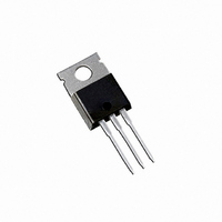
MOSFET N-CH 30V 105A TO-220AB
Manufacturer
International Rectifier
Series
HEXFET®r
Datasheet
1.IRL8113LPBF.pdf
(13 pages)
Specifications of IRL8113PBF
Fet Type
MOSFET N-Channel, Metal Oxide
Fet Feature
Logic Level Gate
Rds On (max) @ Id, Vgs
6 mOhm @ 21A, 10V
Drain To Source Voltage (vdss)
30V
Current - Continuous Drain (id) @ 25° C
105A
Vgs(th) (max) @ Id
2.25V @ 250µA
Gate Charge (qg) @ Vgs
35nC @ 4.5V
Input Capacitance (ciss) @ Vds
2840pF @ 15V
Power - Max
110W
Mounting Type
Through Hole
Package / Case
TO-220-3 (Straight Leads)
Transistor Polarity
N Channel
Continuous Drain Current Id
105A
Drain Source Voltage Vds
30V
On Resistance Rds(on)
6mohm
Rds(on) Test Voltage Vgs
10V
Threshold Voltage Vgs Typ
2.25V
Rohs Compliant
Yes
Resistance Drain-source Rds (on)
7.1 mOhms
Drain-source Breakdown Voltage
30 V
Gate-source Breakdown Voltage
20 V
Continuous Drain Current
105 A
Power Dissipation
110 W
Mounting Style
Through Hole
Gate Charge Qg
23 nC
Lead Free Status / RoHS Status
Lead free / RoHS Compliant
Other names
*IRL8113PBF
Available stocks
Company
Part Number
Manufacturer
Quantity
Price
Company:

Part Number:
IRL8113PBF
Manufacturer:
FAIRCHIL
Quantity:
849
Part Number:
IRL8113PBF
Manufacturer:
INFINEON/英飞凌
Quantity:
20 000


BV
∆ΒV
R
V
∆V
I
I
gfs
Q
Q
Q
t
t
t
t
C
C
C
E
I
E
I
I
V
t
Q
Static @ T
Avalanche Characteristics
Diode Characteristics
DSS
GSS
d(on)
r
d(off)
f
AR
S
SM
rr
2
DS(on)
GS(th)
iss
oss
rss
AS
AR
SD
g
sw
oss
rr
Q
Q
Q
Q
GS(th)
DSS
gs1
gs2
gd
godr
DSS
/∆T
/∆T
J
J
J
Drain-to-Source Breakdown Voltage
Breakdown Voltage Temp. Coefficient
Static Drain-to-Source On-Resistance
Gate Threshold Voltage
Gate Threshold Voltage Coefficient
Drain-to-Source Leakage Current
Gate-to-Source Forward Leakage
Gate-to-Source Reverse Leakage
Forward Transconductance
Total Gate Charge
Pre-Vth Gate-to-Source Charge
Post-Vth Gate-to-Source Charge
Gate-to-Drain Charge
Gate Charge Overdrive
Switch Charge (Q
Output Charge
Turn-On Delay Time
Rise Time
Turn-Off Delay Time
Fall Time
Input Capacitance
Output Capacitance
Reverse Transfer Capacitance
Single Pulse Avalanche Energy
Avalanche Current
Repetitive Avalanche Energy
Continuous Source Current
(Body Diode)
Pulsed Source Current
(Body Diode)
Diode Forward Voltage
Reverse Recovery Time
Reverse Recovery Charge
= 25°C (unless otherwise specified)
Parameter
Ù
Parameter
Parameter
gs2
Ù
+ Q
gd
)
™
Min. Typ. Max. Units
Min. Typ. Max. Units
1.35
–––
–––
–––
–––
–––
–––
–––
–––
–––
–––
–––
–––
–––
–––
–––
–––
–––
–––
–––
–––
–––
–––
–––
–––
–––
–––
–––
30
86
0.020
2840
-5.0
–––
–––
–––
–––
–––
–––
620
290
–––
–––
–––
4.8
5.7
6.0
2.0
8.3
6.7
5.0
7.2
23
10
14
14
38
18
18
105
Typ.
2.25
-100
–––
–––
––– mV/°C
150
100
–––
–––
–––
–––
–––
–––
–––
–––
–––
–––
–––
–––
–––
–––
–––
–––
–––
420
6.0
7.1
1.0
1.0
35
27
11
h
V/°C
mΩ
nC
nC
nC
µA
nA
pF
ns
ns
V
V
S
A
V
V
Reference to 25°C, I
V
V
V
V
V
V
V
V
V
V
I
See Fig. 16
V
V
I
Clamped Inductive Load
V
V
ƒ = 1.0MHz
MOSFET symbol
showing the
integral reverse
p-n junction diode.
T
T
di/dt = 100A/µs
D
D
J
J
GS
GS
GS
DS
DS
DS
GS
GS
DS
DS
GS
DS
DD
GS
DS
= 17A
= 17A
= 25°C, I
= 25°C, I
= 0V, I
= 10V, I
= 4.5V, I
= V
= 24V, V
= 24V, V
= 20V
= -20V
= 15V, I
= 15V
= 4.5V
= 16V, V
= 15V, V
= 0V
= 15V
GS
Max.
220
, I
17
11
D
Conditions
Conditions
D
S
F
D
D
= 250µA
D
GS
GS
GS
GS
= 250µA
= 17A, V
= 17A, V
= 21A
= 17A
= 17A
e
= 0V
= 0V, T
= 0V
= 4.5V
www.irf.com
D
e
e
= 1mA
GS
DD
J
e
G
= 125°C
= 15V
= 0V
Units
mJ
mJ
A
e
D
S
Related parts for IRL8113PBF
Image
Part Number
Description
Manufacturer
Datasheet
Request
R

Part Number:
Description:
MOSFET N-CH 30V 105A TO-220AB
Manufacturer:
International Rectifier
Datasheet:

Part Number:
Description:
SCHOTTKY RECTIFIER
Manufacturer:
International Rectifier Corp.
Datasheet:
Part Number:
Description:
SCHOTTKY RECTIFIER
Manufacturer:
International Rectifier Corp.
Datasheet:
Part Number:
Description:
SCHOTTKY RECTIFIER
Manufacturer:
International Rectifier Corp.
Datasheet:
Part Number:
Description:
SCHOTTKY RECTIFIER
Manufacturer:
International Rectifier Corp.
Datasheet:
Part Number:
Description:
SCHOTTKY RECTIFIER
Manufacturer:
International Rectifier Corp.
Datasheet:
Part Number:
Description:
SCHOTTKY RECTIFIER
Manufacturer:
International Rectifier Corp.
Datasheet:
Part Number:
Description:
SCHOTTKY RECTIFIER
Manufacturer:
International Rectifier Corp.
Datasheet:
Part Number:
Description:
SCHOTTKY RECTIFIER
Manufacturer:
International Rectifier Corp.
Datasheet:
Part Number:
Description:
SCHOTTKY RECTIFIER
Manufacturer:
International Rectifier Corp.
Datasheet:
Part Number:
Description:
SCHOTTKY RECTIFIER
Manufacturer:
International Rectifier Corp.
Datasheet:
Part Number:
Description:
SCHOTTKY RECTIFIER
Manufacturer:
International Rectifier Corp.
Datasheet:
Part Number:
Description:
SCHOTTKY RECTIFIER
Manufacturer:
International Rectifier Corp.
Datasheet:
Part Number:
Description:
SCHOTTKY RECTIFIER
Manufacturer:
International Rectifier Corp.
Datasheet:
Part Number:
Description:
SCHOTTKY RECTIFIER
Manufacturer:
International Rectifier Corp.
Datasheet: