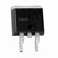
IRF4905SPBF International Rectifier, IRF4905SPBF Datasheet - Page 7

IRF4905SPBF
Manufacturer Part Number
IRF4905SPBF
Description
MOSFET P-CH 55V 42A D2PAK
Manufacturer
International Rectifier
Series
HEXFET®r
Specifications of IRF4905SPBF
Fet Type
MOSFET P-Channel, Metal Oxide
Fet Feature
Standard
Rds On (max) @ Id, Vgs
20 mOhm @ 42A, 10V
Drain To Source Voltage (vdss)
55V
Current - Continuous Drain (id) @ 25° C
42A
Vgs(th) (max) @ Id
4V @ 250µA
Gate Charge (qg) @ Vgs
180nC @ 10V
Input Capacitance (ciss) @ Vds
3500pF @ 25V
Power - Max
170W
Mounting Type
Surface Mount
Package / Case
D²Pak, TO-263 (2 leads + tab)
Channel Type
P
Current, Drain
-70 A
Gate Charge, Total
120 nC
Package Type
D2Pak
Polarization
P-Channel
Power Dissipation
170 W
Resistance, Drain To Source On
0.020 Ohm
Temperature, Operating, Maximum
+150 °C
Temperature, Operating, Minimum
-55 °C
Time, Turn-off Delay
51 ns
Time, Turn-on Delay
20 ns
Transconductance, Forward
19 S
Voltage, Breakdown, Drain To Source
-55 V
Voltage, Drain To Source
–55 V
Voltage, Forward, Diode
-1.3 V
Voltage, Gate To Source
±20 V
Configuration
Single
Transistor Polarity
P-Channel
Resistance Drain-source Rds (on)
20 m Ohms
Drain-source Breakdown Voltage
- 55 V
Gate-source Breakdown Voltage
20 V
Continuous Drain Current
- 74 A
Maximum Operating Temperature
+ 175 C
Mounting Style
SMD/SMT
Fall Time
96 ns
Gate Charge Qg
120 nC
Minimum Operating Temperature
- 55 C
Rise Time
99 ns
Lead Free Status / RoHS Status
Lead free / RoHS Compliant
Available stocks
Company
Part Number
Manufacturer
Quantity
Price
Company:
Part Number:
IRF4905SPBF
Manufacturer:
IR
Quantity:
21 000
www.irf.com
1000
100
0.1
10
160
120
1
1.0E-06
80
40
0
Fig 16. Maximum Avalanche Energy
25
Duty Cycle = Single Pulse
Starting T J , Junction Temperature (°C)
0.01
0.05
0.10
50
Vs. Temperature
TOP
BOTTOM 1% Duty Cycle
I D = -42A
1.0E-05
75
Fig 15. Typical Avalanche Current Vs.Pulsewidth
Single Pulse
100
125
1.0E-04
150
tav (sec)
Notes on Repetitive Avalanche Curves , Figures 15, 16:
(For further info, see AN-1005 at www.irf.com)
1. Avalanche failures assumption:
2. Safe operation in Avalanche is allowed as long asT
3. Equation below based on circuit and waveforms shown in
4. P
5. BV = Rated breakdown voltage (1.3 factor accounts for
6. I
7. ∆T
Purely a thermal phenomenon and failure occurs at a
temperature far in excess of T
every part type.
not exceeded.
Figures 12a, 12b.
avalanche pulse.
voltage increase during avalanche).
T
t
D = Duty cycle in avalanche = t
Z
av
av =
thJC
D (ave)
jmax
= Allowable avalanche current.
=
Average time in avalanche.
(D, t
Allowable rise in junction temperature, not to exceed
(assumed as 25°C in Figure 15, 16).
= Average power dissipation per single
av
1.0E-03
P
) = Transient thermal resistance, see figure 11)
D (ave)
Allowed avalanche Current vs
avalanche
assuming ∆Tj = 25°C due to
avalanche losses. Note: In no
case should Tj be allowed to
exceed Tjmax
= 1/2 ( 1.3·BV·I
I
E
av
AS (AR)
= 2DT/ [1.3·BV·Z
= P
D (ave)
jmax
pulsewidth,
1.0E-02
av
av
. This is validated for
·f
) = DT/ Z
·t
th
av
]
thJC
tav
jmax
1.0E-01
7
is


