STP80NF55-06FP STMicroelectronics, STP80NF55-06FP Datasheet - Page 3
STP80NF55-06FP
Manufacturer Part Number
STP80NF55-06FP
Description
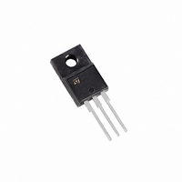
MOSFET N-CH 55V 60A TO-220FP
Manufacturer
STMicroelectronics
Series
STripFET™r
Specifications of STP80NF55-06FP
Fet Type
MOSFET N-Channel, Metal Oxide
Fet Feature
Standard
Rds On (max) @ Id, Vgs
6.5 mOhm @ 40A, 10V
Drain To Source Voltage (vdss)
55V
Current - Continuous Drain (id) @ 25° C
60A
Vgs(th) (max) @ Id
4V @ 250µA
Gate Charge (qg) @ Vgs
189nC @ 10V
Input Capacitance (ciss) @ Vds
4400pF @ 25V
Power - Max
45W
Mounting Type
Through Hole
Package / Case
TO-220FP
Transistor Polarity
N Channel
Continuous Drain Current Id
60A
Drain Source Voltage Vds
55V
On Resistance Rds(on)
5mohm
Rds(on) Test Voltage Vgs
10V
Threshold Voltage Vgs Typ
3V
Rohs Compliant
Yes
Configuration
Single
Resistance Drain-source Rds (on)
0.0065 Ohms
Drain-source Breakdown Voltage
55 V
Gate-source Breakdown Voltage
+/- 20 V
Continuous Drain Current
60 A
Power Dissipation
45 W
Maximum Operating Temperature
+ 175 C
Mounting Style
Through Hole
Minimum Operating Temperature
- 55 C
Lead Free Status / RoHS Status
Lead free / RoHS Compliant
Available stocks
Company
Part Number
Manufacturer
Quantity
Price
Company:

Part Number:
STP80NF55-06FP
Manufacturer:
ST
Quantity:
12 500
Part Number:
STP80NF55-06FP
Manufacturer:
ST
Quantity:
20 000


ELECTRICAL CHARACTERISTICS (continued)
SWITCHING ON
SWITCHING OFF
SOURCE DRAIN DIODE
(*)
(
Safe Operating Area for TO-220
•)
Pulsed: Pulse duration = 300 µs, duty cycle 1.5 %.
Pulse width limited by safe operating area.
Symbol
Symbol
Symbol
I
V
SDM (
t
t
I
Q
Q
d(on)
d(off)
SD (*)
RRM
I
Q
Q
SD
t
t
t
rr
gs
gd
r
f
rr
g
•
)
Turn-on Delay Time
Rise Time
Total Gate Charge
Gate-Source Charge
Gate-Drain Charge
Turn-off Delay Time
Fall Time
Source-drain Current
Source-drain Current (pulsed)
Forward On Voltage
Reverse Recovery Time
Reverse Recovery Charge
Reverse Recovery Current
Parameter
Parameter
Parameter
V
(Resistive Load, Figure 3)
V
V
R
(Resistive Load, Figure 3)
I
I
V
(see test circuit, Figure 5)
SD
SD
R
DD
DD
DD
DD
G
STB80NF55-06/-1 STP80NF55-06 STP80NF55-06FP
G
= 4.7 Ω,
= 80 A
= 80 A
= 44 V I
= 27 V
= 27 V
= 35 V
= 4.7 Ω
Test Conditions
Test Conditions
Test Conditions
D
= 80 A V
Safe Operating Area for TO-220FP
di/dt = 100A/µs
V
V
V
T
GS
GS
GS
j
I
I
= 150°C
D
D
GS
= 0
= 10 V
= 40 A
= 10 V
= 40 A
= 10V
Min.
Min.
Min.
Typ.
60.5
Typ.
Typ.
0.32
155
142
125
100
6.5
27
29
65
Max.
Max.
Max.
193
320
1.5
80
Unit
Unit
Unit
nC
nC
nC
µ C
ns
ns
ns
ns
ns
A
A
V
A
3/12
Related parts for STP80NF55-06FP
Image
Part Number
Description
Manufacturer
Datasheet
Request
R

Part Number:
Description:
MOSFET N-CH 55V 80A TO-220
Manufacturer:
STMicroelectronics
Datasheet:
Part Number:
Description:
MOSFET N-CH 55V 80A TO-220
Manufacturer:
STMicroelectronics
Datasheet:

Part Number:
Description:
N-CHANNEL 55V - 0.005 Ohms - 80A TO-220FP STripFET POWER MOSFET
Manufacturer:
STMicroelectronics
Part Number:
Description:
N-CHANNEL 55V - 0.0055 OMH - 80A - TO-220 STRIPFET POWER MOSFET
Manufacturer:
STMicroelectronics
Part Number:
Description:
STMicroelectronics [RIPPLE-CARRY BINARY COUNTER/DIVIDERS]
Manufacturer:
STMicroelectronics
Datasheet:
Part Number:
Description:
STMicroelectronics [LIQUID-CRYSTAL DISPLAY DRIVERS]
Manufacturer:
STMicroelectronics
Datasheet:

Part Number:
Description:
BOARD EVAL FOR MEMS SENSORS
Manufacturer:
STMicroelectronics
Datasheet:
Part Number:
Description:
NPN TRANSISTOR POWER MODULE
Manufacturer:
STMicroelectronics
Datasheet:
Part Number:
Description:
TURBOSWITCH ULTRA-FAST HIGH VOLTAGE DIODE
Manufacturer:
STMicroelectronics
Datasheet:
Part Number:
Description:
Manufacturer:
STMicroelectronics
Datasheet:
Part Number:
Description:
DIODE / SCR MODULE
Manufacturer:
STMicroelectronics
Datasheet: