STF11NM50N STMicroelectronics, STF11NM50N Datasheet - Page 4
STF11NM50N
Manufacturer Part Number
STF11NM50N
Description
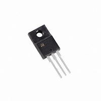
MOSFET N-CH 500V 9A TO-220FP
Manufacturer
STMicroelectronics
Series
MDmesh™r
Datasheet
1.STF11NM50N.pdf
(16 pages)
Specifications of STF11NM50N
Fet Type
MOSFET N-Channel, Metal Oxide
Fet Feature
Standard
Rds On (max) @ Id, Vgs
470 mOhm @ 4.5A, 10V
Drain To Source Voltage (vdss)
500V
Current - Continuous Drain (id) @ 25° C
8.5A
Vgs(th) (max) @ Id
4V @ 250µA
Gate Charge (qg) @ Vgs
19nC @ 10V
Input Capacitance (ciss) @ Vds
547pF @ 50V
Power - Max
25W
Mounting Type
Through Hole
Package / Case
TO-220FP
Lead Free Status / RoHS Status
Lead free / RoHS Compliant
Available stocks
Company
Part Number
Manufacturer
Quantity
Price
Company:

Part Number:
STF11NM50N
Manufacturer:
STMicroelectronics
Quantity:
800
Part Number:
STF11NM50N
Manufacturer:
ST
Quantity:
20 000


Electrical characteristics
2
4/16
Electrical characteristics
(T
Table 4.
Table 5.
1. C
2. C
V
Symbol
Symbol
C
C
R
C
V
(BR)DSS
when V
C
C
o(er)
I
I
C
DS(on)
C
o(tr)
Q
GS(th)
Q
= 25 °C unless otherwise specified)
GSS
R
DSS
Q
oss eq.
oss eq.
oss
oss
iss
rss
gs
gd
G
g
(1)
(2)
when V
DS
time related is defined as a constant equivalent capacitance giving the same charging time as C
energy related is defined as a constant equivalent capacitance giving the same stored energy as
Input capacitance
Output capacitance
Reverse transfer
capacitance
Equivalent
capacitance time
related
Equivalent
capacitance energy
related
Intrinsic gate
resistance
Total gate charge
Gate-source charge
Gate-drain charge
increases from 0 to 80% V
Drain-source
breakdown voltage
Zero gate voltage
drain current (V
Gate-body leakage
current (V
Gate threshold voltage V
Static drain-source on
resistance
On /off states
Dynamic
DS
increases from 0 to 80% V
Parameter
Parameter
DS
= 0)
GS
= 0)
Doc ID 17156 Rev 1
DSS
V
V
V
f = 1 MHz open drain
V
V
(see
I
V
V
V
V
D
DS
GS
DS
DD
GS
DS
DS
GS
DS
GS
= 1 mA, V
DSS
= Max rating
= Max rating, T
= 50 V, f = 1 MHz,
= 0
= 0 to 400 V, V
= 10 V
= ± 25 V
= V
= 10 V, I
= 400 V, I
Figure
Test conditions
Test conditions
GS
, I
18)
STD11NM50N, STF11NM50N, STP11NM50N
GS
D
D
D
= 250 µA
= 4.5 A
= 0
= 9 A,
GS
C
=125 °C
= 0
Min.
Min.
500
2
-
-
-
-
-
Typ.
Typ.
547
5.8
3.7
0.4
42
59
29
19
10
3
2
Max.
Max.
0.47
100
10
1
4
-
-
-
-
-
oss
Unit
Unit
nC
nC
nC
µA
µA
nA
pF
pF
pF
pF
pF
Ω
Ω
V
V
Related parts for STF11NM50N
Image
Part Number
Description
Manufacturer
Datasheet
Request
R

Part Number:
Description:
STMicroelectronics [RIPPLE-CARRY BINARY COUNTER/DIVIDERS]
Manufacturer:
STMicroelectronics
Datasheet:
Part Number:
Description:
STMicroelectronics [LIQUID-CRYSTAL DISPLAY DRIVERS]
Manufacturer:
STMicroelectronics
Datasheet:

Part Number:
Description:
BOARD EVAL FOR MEMS SENSORS
Manufacturer:
STMicroelectronics
Datasheet:
Part Number:
Description:
NPN TRANSISTOR POWER MODULE
Manufacturer:
STMicroelectronics
Datasheet:
Part Number:
Description:
TURBOSWITCH ULTRA-FAST HIGH VOLTAGE DIODE
Manufacturer:
STMicroelectronics
Datasheet:
Part Number:
Description:
Manufacturer:
STMicroelectronics
Datasheet:
Part Number:
Description:
DIODE / SCR MODULE
Manufacturer:
STMicroelectronics
Datasheet:
Part Number:
Description:
DIODE / SCR MODULE
Manufacturer:
STMicroelectronics
Datasheet:
Part Number:
Description:
Search -----> STE16N100
Manufacturer:
STMicroelectronics
Datasheet:
Part Number:
Description:
Search ---> STE53NA50
Manufacturer:
STMicroelectronics
Datasheet:
Part Number:
Description:
NPN Transistor Power Module
Manufacturer:
STMicroelectronics
Datasheet:
Part Number:
Description:
DIODE / SCR MODULE
Manufacturer:
STMicroelectronics
Datasheet: