IRF3315SPBF International Rectifier, IRF3315SPBF Datasheet - Page 2
IRF3315SPBF
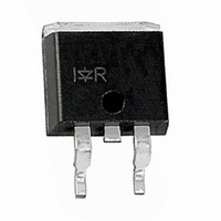
Manufacturer Part Number
IRF3315SPBF
Description
MOSFET N-CH 150V 21A D2PAK
Manufacturer
International Rectifier
Series
HEXFET®r
Specifications of IRF3315SPBF
Fet Type
MOSFET N-Channel, Metal Oxide
Fet Feature
Standard
Rds On (max) @ Id, Vgs
82 mOhm @ 12A, 10V
Drain To Source Voltage (vdss)
150V
Current - Continuous Drain (id) @ 25° C
21A
Vgs(th) (max) @ Id
4V @ 250µA
Gate Charge (qg) @ Vgs
95nC @ 10V
Input Capacitance (ciss) @ Vds
1300pF @ 25V
Power - Max
3.8W
Mounting Type
Surface Mount
Package / Case
D²Pak, TO-263 (2 leads + tab)
Current, Drain
21 A
Gate Charge, Total
95 nC
Package Type
D2Pak
Polarization
N-Channel
Power Dissipation
94 W
Resistance, Drain To Source On
0.082 Ohm
Temperature, Operating, Maximum
+175 °C
Temperature, Operating, Minimum
-55 °C
Time, Turn-off Delay
49 ns
Time, Turn-on Delay
9.6 ns
Transconductance, Forward
17 S
Voltage, Breakdown, Drain To Source
150 V
Voltage, Forward, Diode
1.3 V
Voltage, Gate To Source
±20 V
Transistor Polarity
N Channel
Continuous Drain Current Id
21A
Drain Source Voltage Vds
150V
On Resistance Rds(on)
82mohm
Rds(on) Test Voltage Vgs
10V
Threshold Voltage Vgs Typ
4V
Rohs Compliant
Yes
Drain-source Breakdown Voltage
150 V
Gate-source Breakdown Voltage
20 V
Continuous Drain Current
21 A
Mounting Style
SMD/SMT
Gate Charge Qg
63.3 nC
Lead Free Status / RoHS Status
Lead free / RoHS Compliant
Other names
*IRF3315SPBF


IRF3315S/L
** When mounted on 1" square PCB ( FR-4 or G-10 Material ).
Electrical Characteristics @ T
Source-Drain Ratings and Characteristics
Notes:
I
I
L
V
R
V
g
Q
Q
Q
t
t
t
t
C
C
C
I
I
V
t
Q
t
DSS
GSS
S
on
d(on)
d(off)
f
SM
r
rr
S
V
For recommended footprint and soldering techniques refer to application note #AN-994.
fs
(BR)DSS
GS(th)
oss
SD
DS(on)
g
gs
gd
iss
rss
rr
V
R
(BR)DSS
Repetitive rating; pulse width limited by
I
T
max. junction temperature. ( See fig. 11 )
SD
DD
J
G
= 25 , I
= 25V, starting T
175°C
12A, di/dt
/ T
J
Drain-to-Source Leakage Current
Internal Source Inductance
Drain-to-Source Breakdown Voltage
Breakdown Voltage Temp. Coefficient
Static Drain-to-Source On-Resistance
Gate Threshold Voltage
Forward Transconductance
Gate-to-Source Forward Leakage
Gate-to-Source Reverse Leakage
Total Gate Charge
Gate-to-Source Charge
Gate-to-Drain ("Miller") Charge
Turn-On Delay Time
Rise Time
Turn-Off Delay Time
Fall Time
Input Capacitance
Output Capacitance
Reverse Transfer Capacitance
Continuous Source Current
(Body Diode)
Pulsed Source Current
(Body Diode)
Diode Forward Voltage
Reverse Recovery Time
Reverse Recovery Charge
Forward Turn-On Time
AS
= 12A. (See Figure 12)
140A/µs, V
J
= 25°C, L = 4.9 mH
Parameter
Parameter
DD
V
(BR)DSS
J
,
= 25°C (unless otherwise specified)
Pulse width
Uses IRF3315 data and test conditions
150
–––
–––
–––
–––
–––
–––
–––
–––
–––
–––
–––
–––
–––
Min. Typ. Max. Units
––– 0.187 –––
–––
–––
Min. Typ. Max. Units
–––
2.0
17
–––
–––
–––
–––
–––
Intrinsic turn-on time is negligible (turn-on is dominated by L
1300 –––
–––
–––
–––
–––
–––
–––
––– -100
–––
–––
–––
300
160
–––
–––
–––
174
––– 0.082
9.6
1.2
49
38
7.5
32
–––
–––
250
100
–––
–––
–––
–––
–––
–––
–––
260
4.0
1.3
1.7
21
300µs; duty cycle
25
95
11
47
84
V/°C
µA
nA
ns
nH
nC
µC
pF
ns
V
V
A
V
S
MOSFET symbol
T
di/dt = 100A/µs
V
Reference to 25°C, I
V
V
V
V
V
V
V
I
V
V
V
I
R
R
Between lead,
and center of die contact
V
V
ƒ = 1.0MHz, See Fig. 5
showing the
p-n junction diode.
T
integral reverse
D
D
J
J
GS
GS
DS
DS
DS
DS
GS
GS
DS
GS
DD
GS
DS
G
D
= 12A
= 12A
= 25°C, I
= 25°C, I
= 5.1
= 5.9
= V
= 120V, V
= 0V, I
= 10V, I
= 50V, I
= 150V, V
= 20V
= 120V
= 10V, See Fig. 6 and 13
= 0V
= 25V
= -20V
= 75V
2%.
GS
, I
See Fig. 10
D
F
S
D
D
D
= 250µA
= 43A
= 43A, V
Conditions
Conditions
= 250µA
= 12A
= 12A
GS
GS
= 0V, T
= 0V
D
GS
= 1mA
J
= 0V
G
= 125°C
S
+L
D
D
S
)
Related parts for IRF3315SPBF
Image
Part Number
Description
Manufacturer
Datasheet
Request
R

Part Number:
Description:
MOSFET N-CH 150V 27A TO-220AB
Manufacturer:
International Rectifier
Datasheet:

Part Number:
Description:
Common Mode Inductors (Chokes) 5.6uH 10%
Manufacturer:
Vishay
Datasheet:
Part Number:
Description:
Common Mode Inductors (Chokes) 10uH 10%
Manufacturer:
Vishay
Datasheet:

Part Number:
Description:
SCHOTTKY RECTIFIER
Manufacturer:
International Rectifier Corp.
Datasheet:
Part Number:
Description:
SCHOTTKY RECTIFIER
Manufacturer:
International Rectifier Corp.
Datasheet:
Part Number:
Description:
SCHOTTKY RECTIFIER
Manufacturer:
International Rectifier Corp.
Datasheet:
Part Number:
Description:
SCHOTTKY RECTIFIER
Manufacturer:
International Rectifier Corp.
Datasheet:
Part Number:
Description:
SCHOTTKY RECTIFIER
Manufacturer:
International Rectifier Corp.
Datasheet:
Part Number:
Description:
SCHOTTKY RECTIFIER
Manufacturer:
International Rectifier Corp.
Datasheet:
Part Number:
Description:
SCHOTTKY RECTIFIER
Manufacturer:
International Rectifier Corp.
Datasheet:
Part Number:
Description:
SCHOTTKY RECTIFIER
Manufacturer:
International Rectifier Corp.
Datasheet:
Part Number:
Description:
SCHOTTKY RECTIFIER
Manufacturer:
International Rectifier Corp.
Datasheet:
Part Number:
Description:
SCHOTTKY RECTIFIER
Manufacturer:
International Rectifier Corp.
Datasheet:
Part Number:
Description:
SCHOTTKY RECTIFIER
Manufacturer:
International Rectifier Corp.
Datasheet:
Part Number:
Description:
SCHOTTKY RECTIFIER
Manufacturer:
International Rectifier Corp.
Datasheet: