IRFL4315PBF International Rectifier, IRFL4315PBF Datasheet - Page 2
IRFL4315PBF
Manufacturer Part Number
IRFL4315PBF
Description
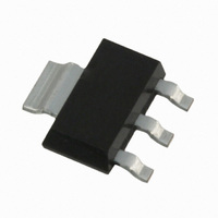
MOSFET N-CH 150V 2.6A SOT223
Manufacturer
International Rectifier
Series
HEXFET®r
Specifications of IRFL4315PBF
Fet Type
MOSFET N-Channel, Metal Oxide
Fet Feature
Standard
Rds On (max) @ Id, Vgs
185 mOhm @ 1.6A, 10V
Drain To Source Voltage (vdss)
150V
Current - Continuous Drain (id) @ 25° C
2.6A
Vgs(th) (max) @ Id
5V @ 250µA
Gate Charge (qg) @ Vgs
19nC @ 10V
Input Capacitance (ciss) @ Vds
420pF @ 25V
Power - Max
2.8W
Mounting Type
Surface Mount
Package / Case
SOT-223 (3 leads + Tab), SC-73, TO-261
Channel Type
N
Current, Drain
2.6 A
Gate Charge, Total
12 nC
Package Type
SOT-223
Polarization
N-Channel
Power Dissipation
2.8 W
Resistance, Drain To Source On
185 Ohm
Temperature, Operating, Maximum
+150 °C
Temperature, Operating, Minimum
-55 °C
Time, Turn-off Delay
20 ns
Time, Turn-on Delay
8.4 ns
Transconductance, Forward
3.5 S
Voltage, Breakdown, Drain To Source
150 V
Voltage, Drain To Source
150 V
Voltage, Forward, Diode
1.5 V
Voltage, Gate To Source
±30 V
Configuration
Single Dual Drain
Transistor Polarity
N-Channel
Resistance Drain-source Rds (on)
185 m Ohms
Drain-source Breakdown Voltage
150 V
Gate-source Breakdown Voltage
30 V
Continuous Drain Current
2.6 A
Maximum Operating Temperature
+ 150 C
Mounting Style
SMD/SMT
Fall Time
19 ns
Gate Charge Qg
12 nC
Minimum Operating Temperature
- 55 C
Rise Time
21 ns
Lead Free Status / RoHS Status
Lead free / RoHS Compliant


Diode Characteristics
IRFL4315PbF
Dynamic @ T
Avalanche Characteristics
Static @ T
E
I
V
R
V
I
I
g
Q
Q
Q
t
t
t
t
C
C
C
C
C
C
I
I
V
t
Q
AR
DSS
GSS
d(on)
r
d(off)
f
S
SM
rr
V
fs
AS
(BR)DSS
DS(on)
GS(th)
SD
iss
oss
rss
oss
oss
oss
g
gs
gd
rr
2
(BR)DSS
eff.
/ T
J
Breakdown Voltage Temp. Coefficient
Drain-to-Source Breakdown Voltage
Static Drain-to-Source On-Resistance
Gate Threshold Voltage
Gate-to-Source Forward Leakage
Gate-to-Source Reverse Leakage
Forward Transconductance
Total Gate Charge
Gate-to-Source Charge
Gate-to-Drain ("Miller") Charge
Turn-On Delay Time
Rise Time
Turn-Off Delay Time
Fall Time
Input Capacitance
Output Capacitance
Reverse Transfer Capacitance
Output Capacitance
Output Capacitance
Effective Output Capacitance
Continuous Source Current
(Body Diode)
Pulsed Source Current
(Body Diode)
Diode Forward Voltage
Reverse Recovery Time
Reverse RecoveryCharge
Drain-to-Source Leakage Current
J
= 25°C (unless otherwise specified)
J
Single Pulse Avalanche Energy‚
Avalanche Current
= 25°C (unless otherwise specified)
Parameter
Parameter
Parameter
Parameter
–––
150
–––
–––
–––
–––
–––
–––
–––
–––
–––
–––
–––
–––
–––
–––
–––
–––
–––
–––
Min. Typ. Max. Units
3.0
Min. Typ. Max. Units
3.5
Min. Typ. Max. Units
–––
–––
–––
–––
–––
0.19 –––
–––
–––
–––
–––
–––
–––
––– -100
–––
420
100
720
–––
–––
–––
160
2.1
6.8
8.4
12
21
20
19
25
48
98
61
–––
185
250
100
–––
–––
–––
–––
–––
–––
–––
–––
–––
–––
–––
240
5.0
3.1
1.5
2.6
25
19
10
91
21
V/°C
m
µA
nA
nC
ns
pF
nC
ns
V
V
S
V
Typ.
–––
–––
V
V
V
V
V
V
V
V
V
V
V
I
R
V
V
V
ƒ = 1.0MHz
V
V
V
MOSFET symbol
showing the
integral reverse
p-n junction diode.
T
T
di/dt = 100A/µs ƒ
Reference to 25°C, I
I
D
D
J
J
GS
GS
DS
DS
DS
GS
GS
DS
DS
GS
DD
G
GS
GS
DS
GS
GS
GS
= 1.6A
= 1.6A
= 25°C, I
= 25°C, I
= 15
= V
= 150V, V
= 120V, V
= 50V, I
= 120V
= 25V
= 0V, I
= 10V, I
= 30V
= -30V
= 10V
= 75V
= 10V ƒ
= 0V
= 0V, V
= 0V, V
= 0V, V
GS
, I
D
S
F
DS
D
D
D
DS
DS
Conditions
= 250µA
Conditions
Conditions
= 2.1A, V
= 1.6A
= 250µA
= 1.6A
= 1.6A
GS
GS
= 0V to 120V …
Max.
= 1.0V, ƒ = 1.0MHz
= 120V, ƒ = 1.0MHz
3.1
38
= 0V, T
= 0V
D
www.irf.com
= 1mA ƒ
GS
ƒ
J
G
= 0V ƒ
= 125°C
Units
mJ
A
S
D
Related parts for IRFL4315PBF
Image
Part Number
Description
Manufacturer
Datasheet
Request
R

Part Number:
Description:
SCHOTTKY RECTIFIER
Manufacturer:
International Rectifier Corp.
Datasheet:
Part Number:
Description:
SCHOTTKY RECTIFIER
Manufacturer:
International Rectifier Corp.
Datasheet:
Part Number:
Description:
SCHOTTKY RECTIFIER
Manufacturer:
International Rectifier Corp.
Datasheet:
Part Number:
Description:
SCHOTTKY RECTIFIER
Manufacturer:
International Rectifier Corp.
Datasheet:
Part Number:
Description:
SCHOTTKY RECTIFIER
Manufacturer:
International Rectifier Corp.
Datasheet:
Part Number:
Description:
SCHOTTKY RECTIFIER
Manufacturer:
International Rectifier Corp.
Datasheet:
Part Number:
Description:
SCHOTTKY RECTIFIER
Manufacturer:
International Rectifier Corp.
Datasheet:
Part Number:
Description:
SCHOTTKY RECTIFIER
Manufacturer:
International Rectifier Corp.
Datasheet:
Part Number:
Description:
SCHOTTKY RECTIFIER
Manufacturer:
International Rectifier Corp.
Datasheet:
Part Number:
Description:
SCHOTTKY RECTIFIER
Manufacturer:
International Rectifier Corp.
Datasheet:
Part Number:
Description:
SCHOTTKY RECTIFIER
Manufacturer:
International Rectifier Corp.
Datasheet:
Part Number:
Description:
SCHOTTKY RECTIFIER
Manufacturer:
International Rectifier Corp.
Datasheet:
Part Number:
Description:
SCHOTTKY RECTIFIER
Manufacturer:
International Rectifier Corp.
Datasheet:
Part Number:
Description:
SCHOTTKY RECTIFIER
Manufacturer:
International Rectifier Corp.
Datasheet:
Part Number:
Description:
SCHOTTKY RECTIFIER
Manufacturer:
International Rectifier Corp.
Datasheet: