BUK7618-55,118 NXP Semiconductors, BUK7618-55,118 Datasheet
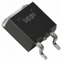
MOSFET N-CH 55V 57A SOT404

BUK7618-55,118

Manufacturer Part Number
BUK7618-55,118
Description
MOSFET N-CH 55V 57A SOT404
Manufacturer
NXP Semiconductors
Series
TrenchMOS™r
Datasheets

Specifications of BUK7618-55,118

Package / Case
D²Pak, TO-263 (2 leads + tab)
Fet Type
MOSFET N-Channel, Metal Oxide
Fet Feature
Standard
Rds On (max) @ Id, Vgs
18 mOhm @ 25A, 10V
Drain To Source Voltage (vdss)
55V
Current - Continuous Drain (id) @ 25° C
57A
Vgs(th) (max) @ Id
4V @ 1mA
Input Capacitance (ciss) @ Vds
2000pF @ 25V
Power - Max
125W
Mounting Type
Surface Mount
Minimum Operating Temperature
- 55 C
Configuration
Single
Transistor Polarity
N-Channel
Resistance Drain-source Rds (on)
0.018 Ohm @ 10 V
Drain-source Breakdown Voltage
55 V
Gate-source Breakdown Voltage
16 V
Continuous Drain Current
57 A
Power Dissipation
125000 mW
Maximum Operating Temperature
+ 175 C
Mounting Style
SMD/SMT
Lead Free Status / RoHS Status
Lead free / RoHS Compliant
Gate Charge (qg) @ Vgs
-
Lead Free Status / Rohs Status
Lead free / RoHS Compliant
Other names
934045250118
BUK7618-55 /T3
BUK7618-55 /T3

Available stocks

Company
Part Number
Manufacturer
Quantity
Price
Part Number:
BUK7618-55,118
Manufacturer:
NEXPERIA/安世
Quantity:
20 000
Philips Semiconductors
GENERAL DESCRIPTION
N-channel
standard level field-effect power
transistor in a plastic envelope
suitable for surface mounting. Using
’trench’
features very low on-state resistance
and has integral zener diodes giving
ESD protection up to 2kV. It is
intended for use in automotive and
general
applications.
PINNING - SOT404
LIMITING VALUES
Limiting values in accordance with the Absolute Maximum System (IEC 134)
ESD LIMITING VALUE
THERMAL RESISTANCES
April 1998
TrenchMOS
Standard level FET
SYMBOL
V
V
I
I
I
P
T
SYMBOL
V
SYMBOL
R
R
D
D
DM
PIN
V
stg
DS
DGR
tot
C
mb
th j-mb
th j-a
1
2
3
GS
, T
j
gate
drain
source
drain
technology
purpose
enhancement
DESCRIPTION
PARAMETER
Drain-source voltage
Drain-gate voltage
Gate-source voltage
Drain current (DC)
Drain current (DC)
Drain current (pulse peak value)
Total power dissipation
Storage & operating temperature
PARAMETER
Electrostatic discharge capacitor
voltage, all pins
PARAMETER
Thermal resistance junction to
mounting base
Thermal resistance junction to
ambient
transistor
the
switching
device
mode
QUICK REFERENCE DATA
PIN CONFIGURATION
SYMBOL
V
I
P
T
R
D
j
DS
tot
DS(ON)
1
2
CONDITIONS
-
R
-
T
T
T
T
-
CONDITIONS
Human body model
(100 pF, 1.5 k )
CONDITIONS
-
Minimum footprint, FR4
board
mb
mb
mb
mb
GS
3
PARAMETER
Drain-source voltage
Drain current (DC)
Total power dissipation
Junction temperature
Drain-source on-state
resistance
= 25 ˚C
= 100 ˚C
= 25 ˚C
= 25 ˚C
= 20 k
1
mb
V
GS
= 10 V
SYMBOL
TYP.
MIN.
MIN.
- 55
50
-
-
-
-
-
-
-
-
-
g
MAX.
Product specification
125
175
55
57
18
MAX.
MAX.
MAX.
228
125
175
1.2
55
55
16
57
40
2
BUK7618-55
-
d
s
Rev 1.000
UNIT
UNIT
UNIT
K/W
K/W
UNIT
kV
W
˚C
m
V
V
V
A
A
A
W
˚C
V
A

Related parts for BUK7618-55,118

BUK7618-55,118 Summary of contents

Page 1

... DS(ON) resistance V GS PIN CONFIGURATION CONDITIONS - ˚ 100 ˚ ˚ ˚ CONDITIONS Human body model (100 pF, 1 CONDITIONS - Minimum footprint, FR4 board 1 Product specification BUK7618-55 MAX. UNIT 55 57 125 175 SYMBOL MIN. MAX. UNIT - 228 - 125 175 ˚C MIN. MAX. UNIT ...

Page 2

... 175˚C j CONDITIONS MHz Resistive load Measured from upper edge of drain tab to centre of die Measured from source lead soldering point to source bond pad CONDITIONS -dI /dt = 100 - Product specification BUK7618-55 MIN. TYP. MAX. UNIT 2.0 3.0 4 500 MIN. ...

Page 3

... RDS(ON) = VDS/ID 120 140 160 180 = f & 0.1 0.01 0.001 120 140 160 180 Product specification BUK7618-55 MIN. TYP. MAX ˚C mb 1000 100 100 1 10 VDS / V Fig.3. Safe operating area ˚ f single pulse; parameter Zth j-mb / (K/ 0.5 0.2 0.1 0.05 0.02 ...

Page 4

... Fig.8. Typical transconductance ˚C . Fig.9. Normalised drain-source on-state resistance -100 Product specification BUK7618- ID f(I ); conditions BUK959-60 Rds(on) normlised to 25degC -100 - 100 Tmb / degC / DS(ON) DS(ON)25 ˚ VGS(TO max. typ. min. - 100 Fig.10. Gate threshold voltage. = f(T ); conditions ...

Page 5

... Sub-Threshold Conduction IF 98 120 110 100 10 100 , Fig.15. Normalised avalanche energy rating. iss oss rss VDS = 44V VGS QG/ Product specification BUK7618-55 Tj/C = 175 0.2 0.4 0.6 0.8 1 VSDS/V Fig.14. Typical reverse diode current. = f(V ); conditions parameter T SDS GS WDSS 100 120 140 Tmb / C ...

Page 6

... Philips Semiconductors TrenchMOS transistor Standard level FET RD VGS RG 0 Fig.17. Switching test circuit. April 1998 VDD + VDS - T.U.T. 6 Product specification BUK7618-55 Rev 1.000 ...

Page 7

... Epoxy meets UL94 V0 at 1/8". April 1998 10.3 max 11 max 15.4 0.85 max (x2) Fig.18. SOT404 : centre pin connected to mounting base. 11.5 9.0 2.0 3.8 5.08 Fig.19. SOT404 : soldering pattern for surface mounting . 7 Product specification BUK7618-55 4.5 max 1.4 max 2.5 0.5 17.5 Rev 1.000 ...

Page 8

... Philips customers using or selling these products for use in such applications their own risk and agree to fully indemnify Philips for any damages resulting from such improper use or sale. April 1998 8 Product specification BUK7618-55 Rev 1.000 ...

Related keywords