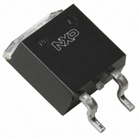
BUK9623-75A,118 NXP Semiconductors, BUK9623-75A,118 Datasheet - Page 5

BUK9623-75A,118
Manufacturer Part Number
BUK9623-75A,118
Description
MOSFET N-CH 75V 53A D2PAK
Manufacturer
NXP Semiconductors
Series
TrenchMOS™r
Specifications of BUK9623-75A,118
Package / Case
D²Pak, TO-263 (2 leads + tab)
Fet Type
MOSFET N-Channel, Metal Oxide
Fet Feature
Logic Level Gate
Rds On (max) @ Id, Vgs
22 mOhm @ 25A, 10V
Drain To Source Voltage (vdss)
75V
Current - Continuous Drain (id) @ 25° C
53A
Vgs(th) (max) @ Id
2V @ 1mA
Input Capacitance (ciss) @ Vds
3120pF @ 25V
Power - Max
138W
Mounting Type
Surface Mount
Minimum Operating Temperature
- 55 C
Configuration
Single
Transistor Polarity
N-Channel
Resistance Drain-source Rds (on)
0.022 Ohm @ 10 V
Drain-source Breakdown Voltage
75 V
Gate-source Breakdown Voltage
+/- 10 V
Continuous Drain Current
53 A
Power Dissipation
138000 mW
Maximum Operating Temperature
+ 175 C
Mounting Style
SMD/SMT
Lead Free Status / RoHS Status
Lead free / RoHS Compliant
Gate Charge (qg) @ Vgs
-
Lead Free Status / Rohs Status
Lead free / RoHS Compliant
Other names
934056476118
BUK9623-75A /T3
BUK9623-75A /T3
BUK9623-75A /T3
BUK9623-75A /T3
8. Characteristics
Table 5:
T
Philips Semiconductors
9397 750 07582
Product specification
Symbol
Static characteristics
V
V
I
I
R
Dynamic characteristics
C
C
C
t
t
t
t
L
L
DSS
GSS
d(on)
r
d(off)
f
j
d
s
(BR)DSS
GS(th)
DSon
iss
oss
rss
= 25 C unless otherwise specified
Characteristics
Parameter
drain-source breakdown
voltage
gate-source threshold voltage I
drain-source leakage current
gate-source leakage current
drain-source on-state
resistance
input capacitance
output capacitance
reverse transfer capacitance
turn-on delay time
rise time
turn-off delay time
fall time
internal drain inductance
internal source inductance
Conditions
I
Figure 9
V
V
V
Figure 7
V
V
V
f = 1 MHz;
V
V
from drain lead 6mm from
package to centre of die
from contact screw on
mounting base to centre of
die SOT78
from upper edge of drain
mounting base to centre of
die SOT404
from source lead to source
bond pad
D
D
DS
GS
GS
GS
GS
GS
DD
GS
T
T
T
T
T
T
T
T
T
T
T
= 0.25 mA; V
= 1 mA; V
j
j
j
j
j
j
j
j
j
j
j
= 75 V; V
= 25 C
= 55 C
= 25 C
= 175 C
= 55 C
= 25 C
= 175 C
= 10 V; V
= 5 V; I
= 25 C
= 175 C
= 4.5 V; I
= 25 C
= 10 V; I
= 25 C
= 0 V; V
= 30 V; R
= 5 V; R
Rev. 01 — 10 October 2000
and
Figure 12
D
BUK9523-75A; BUK9623-75A
DS
DS
G
D
8
= 25 A;
D
GS
L
= 10 ;
= 25 A;
DS
= V
= 25 A;
GS
= 25 V;
= 1.2 ;
= 0 V
= 0 V
= 0 V
GS
;
Min
75
70
1
0.5
TrenchMOS™ logic level FET
Typ
1.5
0.05
2
18
17
2340
319
215
24
141
142
108
4.5
3.5
2.5
7.5
© Philips Electronics N.V. 2000. All rights reserved.
Max
2
2.3
10
500
100
23
49
26
22
3120
383
295
Unit
V
V
V
V
V
nA
m
m
m
m
pF
pF
pF
ns
ns
ns
ns
nH
nH
nH
nH
5 of 15
A
A


