BSS192,115 NXP Semiconductors, BSS192,115 Datasheet - Page 7
BSS192,115
Manufacturer Part Number
BSS192,115
Description
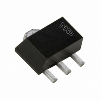
MOSFET P-CH 240V 0.2A SOT89
Manufacturer
NXP Semiconductors
Datasheet
1.BSS192115.pdf
(12 pages)
Specifications of BSS192,115
Package / Case
SC-62, SOT-89, TO-243 (3 Leads + Tab)
Mounting Type
Surface Mount
Power - Max
1W
Fet Type
MOSFET P-Channel, Metal Oxide
Vgs(th) (max) @ Id
2.8V @ 1mA
Current - Continuous Drain (id) @ 25° C
200mA
Drain To Source Voltage (vdss)
240V
Fet Feature
Logic Level Gate
Rds On (max) @ Id, Vgs
12 Ohm @ 200mA, 10V
Minimum Operating Temperature
- 65 C
Configuration
Single
Transistor Polarity
P-Channel
Resistance Drain-source Rds (on)
12 Ohm @ 10 V
Forward Transconductance Gfs (max / Min)
200 mS, 60 mS
Drain-source Breakdown Voltage
240 V
Gate-source Breakdown Voltage
+/- 20 V
Continuous Drain Current
0.2 A
Power Dissipation
1000 mW
Maximum Operating Temperature
+ 150 C
Mounting Style
SMD/SMT
Lead Free Status / RoHS Status
Lead free / RoHS Compliant
Gate Charge (qg) @ Vgs
-
Lead Free Status / Rohs Status
Lead free / RoHS Compliant
Other names
933943950115::BSS192 T/R::BSS192 T/R
Available stocks
Company
Part Number
Manufacturer
Quantity
Price

Part Number:
BSS192,115
Manufacturer:
NEXPERIA/安世
Quantity:
20 000


Philips Semiconductors
PACKAGE OUTLINE
2002 May 22
Plastic surface mounted package; collector pad for good heat transfer; 3 leads
P-channel enhancement mode
vertical D-MOS transistor
DIMENSIONS (mm are the original dimensions)
UNIT
mm
OUTLINE
VERSION
SOT89
1.6
1.4
A
0.48
0.35
b 1
0.53
0.40
b 2
w
IEC
M
1.8
1.4
b 3
0.44
0.37
1
c
b 1
e
1
TO-243
JEDEC
4.6
4.4
D
0
b 3
D
e
REFERENCES
2
2.6
2.4
E
b 2
3.0
e
SC-62
scale
EIAJ
7
2
3
1.5
e 1
B
A
E
L
4.25
3.75
H E
min.
0.8
4 mm
L
0.13
w
PROJECTION
EUROPEAN
c
H E
Product specification
ISSUE DATE
BSS192
97-02-28
99-09-13
SOT89
Related parts for BSS192,115
Image
Part Number
Description
Manufacturer
Datasheet
Request
R

Part Number:
Description:
Intermediate level P-channel enhancement mode Field-Effect Transistor (FET) in a plastic package using vertical D-MOS technology
Manufacturer:
NXP Semiconductors
Datasheet:

Part Number:
Description:
MOSFET P-CH 240V 200MA SOT-89
Manufacturer:
NXP Semiconductors
Datasheet:

Part Number:
Description:
MOSFET TAPE13 PWR-MOS
Manufacturer:
NXP Semiconductors
Datasheet:
Part Number:
Description:
MOSFET TAPE-7 MOSFET
Manufacturer:
NXP Semiconductors
Datasheet:
Part Number:
Description:
NXP Semiconductors designed the LPC2420/2460 microcontroller around a 16-bit/32-bitARM7TDMI-S CPU core with real-time debug interfaces that include both JTAG andembedded trace
Manufacturer:
NXP Semiconductors
Datasheet:

Part Number:
Description:
NXP Semiconductors designed the LPC2458 microcontroller around a 16-bit/32-bitARM7TDMI-S CPU core with real-time debug interfaces that include both JTAG andembedded trace
Manufacturer:
NXP Semiconductors
Datasheet:
Part Number:
Description:
NXP Semiconductors designed the LPC2468 microcontroller around a 16-bit/32-bitARM7TDMI-S CPU core with real-time debug interfaces that include both JTAG andembedded trace
Manufacturer:
NXP Semiconductors
Datasheet:
Part Number:
Description:
NXP Semiconductors designed the LPC2470 microcontroller, powered by theARM7TDMI-S core, to be a highly integrated microcontroller for a wide range ofapplications that require advanced communications and high quality graphic displays
Manufacturer:
NXP Semiconductors
Datasheet:
Part Number:
Description:
NXP Semiconductors designed the LPC2478 microcontroller, powered by theARM7TDMI-S core, to be a highly integrated microcontroller for a wide range ofapplications that require advanced communications and high quality graphic displays
Manufacturer:
NXP Semiconductors
Datasheet:
Part Number:
Description:
The Philips Semiconductors XA (eXtended Architecture) family of 16-bit single-chip microcontrollers is powerful enough to easily handle the requirements of high performance embedded applications, yet inexpensive enough to compete in the market for hi
Manufacturer:
NXP Semiconductors
Datasheet:
Part Number:
Description:
The XA-S3 device is a member of Philips Semiconductors? XA(eXtended Architecture) family of high performance 16-bitsingle-chip microcontrollers
Manufacturer:
NXP Semiconductors
Datasheet:

Part Number:
Description:
The NXP BlueStreak LH75401/LH75411 family consists of two low-cost 16/32-bit System-on-Chip (SoC) devices
Manufacturer:
NXP Semiconductors
Datasheet:
Part Number:
Description:
The NXP LPC3130/3131 combine an 180 MHz ARM926EJ-S CPU core, high-speed USB2
Manufacturer:
NXP Semiconductors
Datasheet:
Part Number:
Description:
The NXP LPC3141 combine a 270 MHz ARM926EJ-S CPU core, High-speed USB 2
Manufacturer:
NXP Semiconductors