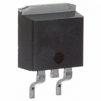
IRFBF20SPBF Vishay, IRFBF20SPBF Datasheet - Page 2

IRFBF20SPBF
Manufacturer Part Number
IRFBF20SPBF
Description
MOSFET N-CH 900V 1.7A D2PAK
Manufacturer
Vishay
Specifications of IRFBF20SPBF
Transistor Polarity
N-Channel
Fet Type
MOSFET N-Channel, Metal Oxide
Fet Feature
Standard
Rds On (max) @ Id, Vgs
8 Ohm @ 1A, 10V
Drain To Source Voltage (vdss)
900V
Current - Continuous Drain (id) @ 25° C
1.7A
Vgs(th) (max) @ Id
4V @ 250µA
Gate Charge (qg) @ Vgs
38nC @ 10V
Input Capacitance (ciss) @ Vds
490pF @ 25V
Power - Max
3.1W
Mounting Type
Surface Mount
Package / Case
D²Pak, TO-263 (2 leads + tab)
Minimum Operating Temperature
- 55 C
Configuration
Single
Resistance Drain-source Rds (on)
8 Ohm @ 10 V
Drain-source Breakdown Voltage
900 V
Gate-source Breakdown Voltage
+/- 20 V
Continuous Drain Current
1.7 A
Power Dissipation
3100 mW
Maximum Operating Temperature
+ 150 C
Mounting Style
SMD/SMT
Continuous Drain Current Id
1.7A
Drain Source Voltage Vds
900V
On Resistance Rds(on)
8ohm
Rds(on) Test Voltage Vgs
10V
Threshold Voltage Vgs Typ
4V
Lead Free Status / RoHS Status
Lead free / RoHS Compliant
Lead Free Status / RoHS Status
Lead free / RoHS Compliant, Lead free / RoHS Compliant
Other names
*IRFBF20SPBF
Available stocks
Company
Part Number
Manufacturer
Quantity
Price
Company:
Part Number:
IRFBF20SPBF
Manufacturer:
Vishay Semiconductors
Quantity:
1 958
Part Number:
IRFBF20SPBF
Manufacturer:
VISHAY/威世
Quantity:
20 000
IRFBF20S, SiHFBF20S, IRFBF20L, SiHFBF20L
Vishay Siliconix
www.vishay.com
2
Note
a. When mounted on 1" square PCB ( FR-4 or G-10 material).
THERMAL RESISTANCE RATINGS
PARAMETER
Maximum Junction-to-Ambient (PCB
Mounted, steady-state)
Maximum Junction-to-Case
SPECIFICATIONS (T
PARAMETER
Static
Drain-Source Breakdown Voltage
V
Gate-Source Threshold Voltage
Gate-Source Leakage
Zero Gate Voltage Drain Current
Drain-Source On-State Resistance
Forward Transconductance
Dynamic
Input Capacitance
Output Capacitance
Reverse Transfer Capacitance
Total Gate Charge
Gate-Source Charge
Gate-Drain Charge
Turn-On Delay Time
Rise Time
Turn-Off Delay Time
Fall Time
DS
Temperature Coefficient
a
J
= 25 °C, unless otherwise noted)
SYMBOL
SYMBOL
V
R
V
C
t
t
I
I
R
R
V
C
C
Q
GS(th)
DS(on)
Q
d(on)
d(off)
GSS
DSS
g
Q
DS
t
DS
oss
t
thJA
thJC
rss
iss
gd
fs
gs
r
f
g
/T
J
V
V
GS
GS
V
R
DS
g
Reference to 25 °C, I
= 10 V
= 10 V
= 18 , V
= 720 V, V
V
V
V
V
V
f = 1.0 MHz, see fig. 5
TYP.
DD
TEST CONDITIONS
DS
DS
DS
GS
-
-
= 450 V, I
= 900 V, V
= V
= 50 V, I
= 0 V, I
V
V
GS
V
GS
DS
GS
GS
I
GS
D
= ± 20 V
= 10 V, see fig. 10
, I
= 25 V,
= 1.7 A, V
= 0 V,
see fig. 6 and 13
= 0 V, T
D
D
D
= 250 μA
D
= 250 μA
I
GS
= 1.0 A
D
= 1.7 A,
= 1.0 A
D
= 0 V
J
= 1 mA
DS
= 125 °C
b
= 360 V,
b
MAX.
b
b
2.3
40
MIN.
900
2.0
0.6
-
-
-
-
-
-
-
-
-
-
-
-
-
-
-
S10-2433-Rev. A, 25-Oct-10
Document Number: 91121
TYP.
490
1.1
8.0
55
18
21
56
32
-
-
-
-
-
-
-
-
-
-
UNIT
°C/W
MAX.
± 100
100
500
8.0
4.7
4.0
38
21
-
-
-
-
-
-
-
-
-
-
mV/°C
UNIT
nA
μA
pF
nC
ns
V
V
S


