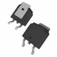
IRFR420APBF Vishay, IRFR420APBF Datasheet

IRFR420APBF
Specifications of IRFR420APBF
Available stocks
Related parts for IRFR420APBF
IRFR420APBF Summary of contents
Page 1
... Typ. ––– 0.50 ––– R (on) max 3.0Ω 3.3A D-Pak I-Pak IRFR420A IRFU420A Max. Units 3.3 2 0.67 W/°C ± 3.4 V/ns Max. Units 140 mJ 2.5 A 5.0 mJ Max. Units 1.5 ––– °C/W 62 www.vishay.com 1 ...
Page 2
... 2. 21Ω G „ 97Ω,See Fig 25V DS pF ƒ = 1.0MHz, See Fig 0V 1.0V, ƒ = 1.0MHz 0V 400V, ƒ = 1.0MHz 400V … 0V Conditions MOSFET symbol showing the integral reverse G p-n junction diode „ 25° 2.5A 25° 2. di/dt = 100A/µs „ DSS www.vishay.com ...
Page 3
... Fig 4. Normalized On-Resistance VGS 15V 10V 8.0V 7.0V 6.0V 5.5V 5.0V 4.5V 4.5V 20µs PULSE WIDTH ° 150 Drain-to-Source Voltage ( 10V 100 120 140 160 ° Junction Temperature ( C) J Vs. Temperature www.vishay.com 100 3 ...
Page 4
... Fig 8. Maximum Safe Operating Area 2. 400V 250V 100V DS FOR TEST CIRCUIT SEE FIGURE Total Gate Charge (nC) G Gate-to-Source Voltage OPERATION IN THIS AREA LIMITED BY R DS(on) 10us 100us 1ms ° 10ms ° = 150 C 100 1000 V , Drain-to-Source Voltage (V) DS www.vishay.com 16 10000 4 ...
Page 5
... Fig 11. Maximum Effective Transient Thermal Impedance, Junction-to-Case Document Number: 91274 Fig 10a. Switching Time Test Circuit V DS 90% 125 150 ° 10 d(on) Fig 10b. Switching Time Waveforms 0.001 0. Rectangular Pulse Duration (sec ≤ 1 ≤ 0 d(off Notes: 1. Duty factor Peak thJC C 0.1 www.vishay.com 1 5 ...
Page 6
... Starting T , Junction Temperature ( C) Fig 12c. Maximum Avalanche Energy 700 650 600 + 550 0.0 Fig 12d. Typical Drain-to-Source Voltage I D TOP 1.1A 1.6A BOTTOM 2. 100 125 ° J Vs. Drain Current 0.5 1.0 1.5 2.0 2 Avalanche Current ( A) Vs. Avalanche Current www.vishay.com 150 6 ...
Page 7
... Voltage Inductor Curent Fig 14. For N-Channel Document Number: 91274 + • • ƒ • - „ • • • • P.W. Period D = Period Body Diode Forward Current di/dt Diode Recovery dv/dt Body Diode Forward Drop Ripple ≤ 5% ® HEXFET Power MOSFETs + - V =10V www.vishay.com 7 ...
Page 8
... INTERNAT IONAL RECTIF IER IRFU120 LOGO 916A SEMBLY LOT CODE PART NUMBER INTERNATIONAL DAT E CODE RECT IFIER IRFU120 P = DESIGNATES LEAD-FREE LOGO PRODUCT (OPTIONAL YEAR 9 = 1999 ASSEMBLY WEEK 16 LOT CODE A = ASSEMBLY SIT E CODE PART NUMBER DATE CODE YEAR 9 = 1999 WEEK 16 LINE A www.vishay.com 8 ...
Page 9
... INT ERNAT IONAL RECT IF IER IRF U120 LOGO 919A SEMBLY LOT CODE PART NUMBER DAT E CODE IRF U120 LOGO P = DES IGNAT ES LEAD-FREE PRODUCT (OPT IONAL YEAR 9 = 1999 ASS EMB LY WEEK 19 LOT CODE SEMB CODE PART NUMBER DAT E CODE YEAR 9 = 1999 WEEK 19 LINE A www.vishay.com 9 ...
Page 10
... Data and specifications subject to change without notice. This product has been designed and qualified for the Industrial market. Qualification Standards can be found on IR’s Web site. TRL TRR 16.3 ( .641 ) 15.7 ( .619 ) FEED DIRECTION 16 mm TAC Fax: (310) 252-7903 12/04 www.vishay.com 10 ...
Page 11
... Except as provided in Vishay's terms and conditions of sale for such products, Vishay assumes no liability whatsoever, and disclaims any express or implied warranty, relating to sale and/or use of Vishay products including liability or warranties relating to fitness for a particular purpose, merchantability, or infringement of any patent, copyright, or other intellectual property right. ...


