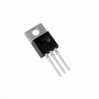
MTP50P03HDLG ON Semiconductor, MTP50P03HDLG Datasheet - Page 5

MTP50P03HDLG
Manufacturer Part Number
MTP50P03HDLG
Description
MOSFET P-CH 30V 50A TO220AB
Manufacturer
ON Semiconductor
Type
Power MOSFETr
Datasheet
1.MTP50P03HDLG.pdf
(8 pages)
Specifications of MTP50P03HDLG
Fet Type
MOSFET P-Channel, Metal Oxide
Fet Feature
Logic Level Gate
Rds On (max) @ Id, Vgs
25 mOhm @ 25A, 5V
Drain To Source Voltage (vdss)
30V
Current - Continuous Drain (id) @ 25° C
50A
Vgs(th) (max) @ Id
2V @ 250µA
Gate Charge (qg) @ Vgs
100nC @ 5V
Input Capacitance (ciss) @ Vds
4900pF @ 25V
Power - Max
125W
Mounting Type
Through Hole
Package / Case
TO-220-3 (Straight Leads)
Configuration
Single
Transistor Polarity
P-Channel
Resistance Drain-source Rds (on)
0.025 Ohm @ 5 V
Forward Transconductance Gfs (max / Min)
20 S
Drain-source Breakdown Voltage
30 V
Gate-source Breakdown Voltage
+/- 15 V
Continuous Drain Current
50 A
Power Dissipation
125000 mW
Maximum Operating Temperature
+ 175 C
Mounting Style
Through Hole
Minimum Operating Temperature
- 55 C
Number Of Elements
1
Polarity
P
Channel Mode
Enhancement
Drain-source On-res
0.025Ohm
Drain-source On-volt
30V
Gate-source Voltage (max)
±15V
Drain Current (max)
50A
Output Power (max)
Not RequiredW
Frequency (max)
Not RequiredMHz
Noise Figure
Not RequireddB
Power Gain
Not RequireddB
Drain Efficiency
Not Required%
Operating Temp Range
-55C to 175C
Operating Temperature Classification
Military
Mounting
Through Hole
Pin Count
3 +Tab
Package Type
TO-220AB
Lead Free Status / RoHS Status
Lead free / RoHS Compliant
Other names
MTP50P03HDLGOS
Available stocks
Company
Part Number
Manufacturer
Quantity
Price
Company:
Part Number:
MTP50P03HDLG
Manufacturer:
FSC
Quantity:
6 000
Part Number:
MTP50P03HDLG
Manufacturer:
ON/安森美
Quantity:
20 000
are very important in systems using it as a freewheeling or
commutating diode. Of particular interest are the reverse
recovery characteristics which play a major role in
determining switching losses, radiated noise, EMI and RFI.
the body diode itself. The body diode is a minority carrier
device, therefore it has a finite reverse recovery time, t
to the storage of minority carrier charge, Q
the typical reverse recovery wave form of Figure 12. It is this
stored charge that, when cleared from the diode, passes
through a potential and defines an energy loss. Obviously,
repeatedly forcing the diode through reverse recovery
further increases switching losses. Therefore, one would
like a diode with short t
minimize these losses.
amount of radiated noise, voltage spikes, and current
ringing. The mechanisms at work are finite irremovable
circuit parasitic inductances and capacitances acted upon by
The switching characteristics of a MOSFET body diode
System switching losses are largely due to the nature of
The abruptness of diode reverse recovery effects the
6
5
4
3
2
1
0
0
Figure 8. Gate−To−Source and Drain−To−Source
Q1
10
Q3
Voltage versus Total Charge
20
Q
T
, TOTAL GATE CHARGE (nC)
30
rr
and low Q
QT
Q2
40
DRAIN−TO−SOURCE DIODE CHARACTERISTICS
50
50
40
30
20
10
0
RR
0.4
Figure 10. Diode Forward Voltage versus Current
V
T
specifications to
J
GS
RR
60
= 25°C
0.6
= 0 V
I
T
D
V
, as shown in
J
V
GS
= 50 A
= 25°C
DS
V
0.8
SD
70
, SOURCE−TO−DRAIN VOLTAGE (VOLTS)
http://onsemi.com
MTP50P03HDL
rr
1.0
, due
80
30
25
20
15
10
5
0
1.2
5
1.4
high di/dts. The diode’s negative di/dt during t
controlled by the device clearing the stored charge.
However, the positive di/dt during t
diode characteristic and is usually the culprit that induces
current ringing. Therefore, when comparing diodes, the
ratio of t
abruptness and thus gives a comparative estimate of
probable noise generated. A ratio of 1 is considered ideal and
values less than 0.5 are considered snappy.
low voltage MOSFETs, high cell density MOSFET diodes
are faster (shorter t
reverse recovery characteristic. The softness advantage of
the high cell density diode means they can be forced through
reverse recovery at a higher di/dt than a standard cell
MOSFET diode without increasing the current ringing or the
noise generated. In addition, power dissipation incurred
from switching the diode will be less due to the shorter
recovery time and lower switching losses.
1000
Compared to ON Semiconductor standard cell density
100
10
1.6
1
V
V
DD
GS
1.8
b
= 30 V
= 10 V
/t
a
Figure 9. Resistive Switching Time
Variation versus Gate Resistance
2.0
serves as a good indicator of recovery
rr
R
2.2
G
), have less stored charge and a softer
I
T
D
, GATE RESISTANCE (Ohms)
J
= 50 A
= 25°C
2.4
t
b
t
d(off)
d(on)
t
t
r
f
is an uncontrollable
a
is directly
10


