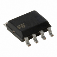
STS2DPFS20V STMicroelectronics, STS2DPFS20V Datasheet

STS2DPFS20V
Specifications of STS2DPFS20V
STS2DPFS20V-E
Available stocks
Related parts for STS2DPFS20V
STS2DPFS20V Summary of contents
Page 1
... Note: For the P-CHANNEL MOSFET actual polarity of voltages and current has to be reversed November 2002 . P-CHANNEL 20V - 0. (@4.5V) 2.5 A (@2.7V) V RRM F(MAX) 0.51 V INTERNAL SCHEMATIC DIAGRAM = kW) = 25° 100° 25° =125 C L =0.5 tp Sinusoidal tp=100 s STS2DPFS20V - 2.5A SO-8 SO-8 Value Unit ± 2 Value Unit ...
Page 2
... STS2DPFS20V TERMAL DATA Rthj-amb (*) Thermal Resistance Junction-ambient MOSFET Rthj-amb (*) Thermal Resistance Junction-ambient SCHOTTKY T Storage Temperature Range stg T Maximum Lead Temperature For Soldering Purpose j (*) 2 When Mounted on 1 inch FR-4 board and t ELECTRICAL CHARACTERISTICS (T OFF Symbol Parameter Drain-source V (BR)DSS Breakdown Voltage Zero Gate Voltage ...
Page 3
... Load, Figure 10V =4. Test Conditions Min 4 4 (Resistive Load, Figure 3) Test Conditions Min di/dt = 100A/µ 150° (see test circuit, Figure 5) Thermal Impedance STS2DPFS20V Typ. Max. Unit 3.5 4.7 nC 0.34 nC 0.8 nC Typ. Max. Unit Typ. Max. Unit 1 7 3/8 ...
Page 4
... STS2DPFS20V Output Characteristics Transconductance Gate Charge vs Gate-source Voltage 4/8 Transfer Characteristics Static Drain-source On Resistance Capacitance Variations ...
Page 5
... Normalized Gate Threshold Voltage vs Temperature Source-drain Diode Forward Characteristics . Normalized on Resistance vs Temperature Normalized Breakdown Voltage vs Temperature. . STS2DPFS20V 5/8 ...
Page 6
... STS2DPFS20V Fig. 1: Unclamped Inductive Load Test Circuit Fig. 1: Unclamped Inductive Load Test Circuit Fig. 3: Switching Times Test Circuits For Resistive Load Fig. 5: Test Circuit For Inductive Load Switching And Diode Recovery Times 6/8 Fig. 2: Unclamped Inductive Waveform Fig. 4: Gate Charge test Circuit ...
Page 7
... STS2DPFS20V MAX. 0.068 0.009 0.064 0.033 0.018 0.010 0.019 0.196 0.244 0.157 0.050 0.023 0016023 7/8 ...
Page 8
... STS2DPFS20V Information furnished is believed to be accurate and reliable. However, STMicroelectronics assumes no responsibility for the consequences of use of such information nor for any infringement of patents or other rights of third parties which may result from its use. No license is granted by implication or otherwise under any patent or patent rights of STMicroelectronics. Specifications mentioned in this publication are subject to change without notice ...


