IXFK110N07 IXYS, IXFK110N07 Datasheet
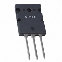
MOSFET N-CH 70V 110A TO-264AA

IXFK110N07

Manufacturer Part Number
IXFK110N07
Description
MOSFET N-CH 70V 110A TO-264AA
Manufacturer
IXYS
Series
HiPerFET™r
Datasheet

Specifications of IXFK110N07

Fet Type
MOSFET N-Channel, Metal Oxide
Fet Feature
Standard
Rds On (max) @ Id, Vgs
6 mOhm @ 500mA, 10V
Drain To Source Voltage (vdss)
70V
Current - Continuous Drain (id) @ 25° C
110A
Vgs(th) (max) @ Id
4V @ 8mA
Gate Charge (qg) @ Vgs
480nC @ 10V
Input Capacitance (ciss) @ Vds
9000pF @ 25V
Power - Max
500W
Mounting Type
Through Hole
Package / Case
TO-264AA
Vdss, Max, (v)
70
Id(cont), Tc=25°c, (a)
110
Rds(on), Max, Tj=25°c, (?)
0.006
Ciss, Typ, (pf)
9000
Qg, Typ, (nc)
480
Trr, Typ, (ns)
-
Trr, Max, (ns)
150
Pd, (w)
500
Rthjc, Max, (ºc/w)
0.25
Package Style
TO-264
Lead Free Status / RoHS Status
Lead free / RoHS Compliant

Available stocks

Company
Part Number
Manufacturer
Quantity
Price
Part Number:
IXFK110N07
Manufacturer:
IXYS
Quantity:
200
© 2000 IXYS All rights reserved
HiPerFET
Power MOSFETs
N-Channel Enhancement Mode
Avalanche Rated, High dv/dt, Low t
Symbol
V
V
V
V
I
I
I
I
E
E
dv/dt
P
T
T
T
T
M
Weight
Symbol
V
V
I
I
R
IXYS reserves the right to change limits, test conditions, and dimensions.
D25
D130
DM
AR
GSS
DSS
J
JM
stg
L
DGR
AR
AS
D
GS (th)
DSS
GS
GSM
DSS
DS(on)
d
T
T
Continuous
Transient
T
T
T
T
T
T
I
T
T
1.6 mm (0.063 in) from case for 10 s
Mounting torque
Terminal connection torque
V
V
V
V
V
V
Note 2
S
J
J
C
C
C
C
C
C
J
C
GS
DS
GS
DS
GS
GS
£ I
= 25°C to 150°C
= 25°C to 150°C; R
£ 150°C, R
= 25°C, die capability
= 130°C, limited by external leads
= 25°C, pulse width limited by T
= 25°C
= 25°C
= 25°C
= 25°C
Test Conditions
Test Conditions
DM
, di/dt £ 100 A/ms, V
= 0 V, I
= V
= ±20 V
= 0.8 • V
= 0 V
= 10 V, I
TM
GS
, I
G
= 2 W
D
D
DC
D
= 1 mA
DSS
= 8 mA
, V
= 0.5 • I
DS
GS
= 0
= 1 MW
D25
DD
£ V
DSS
T
T
110N06/110N07
105N07
J
J
JM
,
(T
= 25°C
= 125°C
N06
N07
rr
J
= 25°C, unless otherwise specified)
N07
N06
N07
N06
min.
-55 ... +150
-55 ... +150
60
70
IXFK 110 N06
IXFK 105 N07
IXFK 110 N07
Characteristic Values
2
Maximum Ratings
0.9/6
typ.
±20
±30
110
100
600
500
150
300
70
60
70
60
76
30
10
2
5
-
max.
±200
400
Nm/lb.in.
Nm/lb.in.
4
2 mA
6 mW
7 mW
V/ns
mJ
nA
mA
°C
°C
°C
°C
W
V
V
V
V
V
V
A
A
A
A
V
V
V
J
g
TO-264 AA (IXFK)
Features
• International standard packages
• JEDEC TO-264 AA, epoxy meet
• Low R
• Rugged polysilicon gate cell structure
• Unclamped Inductive Switching (UIS)
• Low package inductance
• Fast intrinsic Rectifier
Applications
• DC-DC converters
• Synchronous rectification
• Battery chargers
• Switched-mode and resonant-mode
• DC choppers
• Temperature and lighting controls
• Low voltage relays
Advantages
• Easy to mount
• Space savings
• High power density
60 V
70 V
70 V
V
t
UL 94 V-0, flammability classification
rated
power supplies
DSS
rr
£ 250 ns
G
DS (on)
D
S
110 A
105 A
110 A
HDMOS
I
D25
TM
process
6 mW
7 mW
6 mW
92802I (10/97)
R
(TAB)
DS(on)
1 - 4

Related parts for IXFK110N07

IXFK110N07 Summary of contents

Page 1

... V = 0.8 • V DSS DS DSS 0.5 • I DS(on Note 2 IXYS reserves the right to change limits, test conditions, and dimensions. © 2000 IXYS All rights reserved IXFK 110 N06 IXFK 105 N07 IXFK 110 N07 rr Maximum Ratings N07 70 N06 60 N07 70 N06 60 ±20 ±30 ...

Page 2

... D25 240 0.25 0.15 Characteristic Values (T = 25°C, unless otherwise specified) J min. typ. max. 110N06/110N07 105N07 110N06/110N07 JM 105N07 150 IXYS MOSFETS and IGBTs are covered by one or more of the following U.S. patents: 4,835,592 4,881,106 5,017,508 4,850,072 4,931,844 5,034,796 TO-264 AA Outline Dim. Millimeter Min ...

Page 3

... V - Volts GS Figure 3. Admittance Curves 1 1.3 1.2 1 10V GS 1.0 0.9 0.8 0 100 200 300 I - Amperes D Figure 5. R normalized to 0.5 I DS(on) © 2000 IXYS All rights reserved IXFK 110N06 IXFK 105N07 IXFK 110N07 V =10V 1.5 2 =150 =100 15V GS 400 500 600 value D25 ...

Page 4

... Coss 4000 2000 Volts DS Figure 9. Capacitance Curves © 2000 IXYS All rights reserved IXFK 110N06 IXFK 105N07 IXFK 110N07 125 100 500 600 700 400 F = 1MHz 300 200 100 Crss 30 40 Figure 10. Source-Drain Voltage vs. Source Current -2 10 Time - Seconds Figure 11 ...

Related keywords