IXTA3N100D2 IXYS, IXTA3N100D2 Datasheet - Page 2
IXTA3N100D2
Manufacturer Part Number
IXTA3N100D2
Description
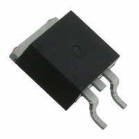
MOSFET N-CH 1000V 3A D2PAK
Manufacturer
IXYS
Datasheet
1.IXTA3N100D2.pdf
(5 pages)
Specifications of IXTA3N100D2
Fet Type
MOSFET N-Channel, Metal Oxide
Fet Feature
Depletion Mode
Rds On (max) @ Id, Vgs
5.5 Ohm @ 1.5A, 0V
Drain To Source Voltage (vdss)
1000V (1kV)
Current - Continuous Drain (id) @ 25° C
3A
Gate Charge (qg) @ Vgs
37.5nC @ 5V
Input Capacitance (ciss) @ Vds
1020pF @ 25V
Power - Max
125W
Mounting Type
Surface Mount
Package / Case
D²Pak, TO-263 (2 leads + tab)
Vds, Max, (v)
1000
Id(on), Min, (a)
3
Rds(on), Max, (?)
5.5
Vgs(off), Max, (v)
-4.5
Ciss, Typ, (pf)
1020
Crss, Typ, (pf)
17
Qg, Typ, (nc)
37.5
Pd, (w)
125
Rthjc, Max, (ºc/w)
1
Package Style
TO-263
Lead Free Status / RoHS Status
Lead free / RoHS Compliant
Vgs(th) (max) @ Id
-


Symbol
(T
g
C
C
C
t
t
t
t
Q
Q
Q
R
R
Safe-Operating-Area Specification
Symbol
SOA
Source-Drain Diode
Symbol
(T
V
t
I
Q
Note 1. Pulse test, t ≤ 300μs, duty cycle, d ≤ 2%.
IXYS Reserves the Right to Change Limits, Test Conditions, and Dimensions.
IXYS MOSFETs and IGBTs are covered
by one or more of the following U.S. patents: 4,850,072
RM
d(on)
r
d(off)
f
rr
fs
SD
iss
oss
rss
thJC
thCS
g(on)
gs
gd
RM
J
J
The product presented herein is under development. The Technical Specifications offered are derived
from data gathered during objective characterizations of preliminary engineering lots; but also may yet
contain some information supplied during a pre-production design evaluation. IXYS reserves the right
to change limits, test conditions, and dimensions without notice.
= 25°C, Unless Otherwise Specified)
= 25°C, Unless Otherwise Specified)
V
V
Resistive Switching Times
V
R
V
TO-220
Test Conditions
V
I
I
V
Test Conditions
Test Conditions
F
F
DS
GS
GS
GS
DS
R
G
= 3A, V
= 3A, -di/dt = 100A/μs
= 100V, V
PRELIMINARY TECHNICAL INFORMATION
= 30V, I
= -10V, V
= ± 5V, V
= 3.3Ω (External)
= 5V, V
= 800V, I
GS
DS
D
= -10V, Note 1
GS
= 1.5A, Note 1
DS
DS
D
= 500V, I
= 94mA, T
= -10V
4,835,592
4,881,106
= 500V, I
= 25V, f = 1MHz
D
4,931,844
5,017,508
5,034,796
= 1.5A
D
C
= 1.5A
= 75°C, Tp = 5s
5,049,961
5,063,307
5,187,117
5,237,481
5,381,025
5,486,715
Characteristic Values
1.2
Min.
Characteristic Values
Characteristic Values
Min.
Min.
75
6,162,665
6,259,123 B1
6,306,728 B1
1020
37.5
21.2
0.50
Typ.
12.7
6.16
2.0
4.4
970
Typ.
Typ.
68
17
27
67
34
40
0.8
Max.
1.0 °C/W
6,404,065 B1
6,534,343
6,583,505
Max.
Max.
1.3
°C/W
nC
nC
nC
μC
pF
pF
pF
ns
ns
ns
ns
ns
W
S
V
A
6,683,344
6,710,405 B2 6,759,692
6,710,463
TO-263 (IXTA) Outline
TO-220 (IXTP) Outline
Pins: 1 - Gate
6,727,585
6,771,478 B2 7,071,537
Dim.
A
b
b2
c
c2
D
D1
E
E1
e
L
L1
L2
L3
L4
3 - Source
14.61
4.06
0.51
1.14
0.40
1.14
8.64
8.00
9.65
6.22
2.54
2.29
1.02
1.27
Min.
Millimeter
0
7,005,734 B2
7,063,975 B2
IXTA3N100D2
IXTP3N100D2
10.41
15.88
Max.
4.83
0.99
1.40
0.74
1.40
9.65
8.89
8.13
BSC
2.79
1.40
1.78
0.13
1. Gate
2. Drain
3. Source
4. Drain
Side
Bottom
2 - Drain
4 - Drain
Min.
.160
.020
.045
.016
.045
.340
.280
.380
.270
.100
.575
.090
.040
.050
7,157,338B2
Inches
0
Max.
BSC
.190
.039
.055
.029
.055
.380
.320
.405
.320
.625
.110
.055
.070
.005
Related parts for IXTA3N100D2
Image
Part Number
Description
Manufacturer
Datasheet
Request
R


Part Number:
Description:
HiPerFET Power MOSFETs
Manufacturer:
IXYS Corporation
Datasheet:
Part Number:
Description:
J-K-Type Flip-Flop
Manufacturer:
IXYS Corporation
Datasheet:
Part Number:
Description:
HiPerRF Power MOSFETs
Manufacturer:
IXYS Corporation
Datasheet:
Part Number:
Description:
Rectifier Module for Three Phase Power Factor Correction
Manufacturer:
IXYS Corporation
Datasheet:
Part Number:
Description:
Thyristor Modules Thyristor/Diode Modules
Manufacturer:
IXYS Corporation
Datasheet:
Part Number:
Description:
Thyristor Modules Thyristor/Diode Modules
Manufacturer:
IXYS Corporation
Datasheet:
Part Number:
Description:
Thyristor Modules Thyristor/Diode Modules
Manufacturer:
IXYS Corporation
Datasheet:
Part Number:
Description:
Thyristor Modules Thyristor/Diode Modules
Manufacturer:
IXYS Corporation
Datasheet:
Part Number:
Description:
Thyristor Modules /Diode Modules
Manufacturer:
IXYS Corporation
Datasheet:
Part Number:
Description:
Thyristor Modules /Diode Modules
Manufacturer:
IXYS Corporation
Datasheet:
Part Number:
Description:
Thyristor Modules Thyristor/Diode Modules
Manufacturer:
IXYS Corporation
Datasheet: