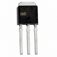
IRLU3303PBF International Rectifier, IRLU3303PBF Datasheet - Page 4

IRLU3303PBF
Manufacturer Part Number
IRLU3303PBF
Description
MOSFET N-CH 30V 35A I-PAK
Manufacturer
International Rectifier
Series
HEXFET®r
Datasheet
1.IRLR3303TRPBF.pdf
(11 pages)
Specifications of IRLU3303PBF
Fet Type
MOSFET N-Channel, Metal Oxide
Fet Feature
Logic Level Gate
Rds On (max) @ Id, Vgs
31 mOhm @ 21A, 10V
Drain To Source Voltage (vdss)
30V
Current - Continuous Drain (id) @ 25° C
35A
Vgs(th) (max) @ Id
1V @ 250µA
Gate Charge (qg) @ Vgs
26nC @ 4.5V
Input Capacitance (ciss) @ Vds
870pF @ 25V
Power - Max
68W
Mounting Type
Through Hole
Package / Case
IPak, TO-251, DPak, VPak (3 straight leads + tab)
Transistor Polarity
N Channel
Continuous Drain Current Id
35A
Drain Source Voltage Vds
30V
On Resistance Rds(on)
31mohm
Rds(on) Test Voltage Vgs
10V
Peak Reflow Compatible (260 C)
Yes
Rohs Compliant
Yes
Resistance Drain-source Rds (on)
45 mOhms
Drain-source Breakdown Voltage
30 V
Gate-source Breakdown Voltage
16 V
Continuous Drain Current
33 A
Power Dissipation
57 W
Mounting Style
SMD/SMT
Gate Charge Qg
17.3 nC
Lead Free Status / RoHS Status
Lead free / RoHS Compliant
Other names
*IRLU3303PBF
1000
4
100
1600
1400
1200
1000
10
800
600
400
200
1
0.0
0
Fig 5. Typical Capacitance Vs.
Fig 7. Typical Source-Drain Diode
1
Drain-to-Source Voltage
T = 175°C
V
C
C
C
J
V
SD
iss
oss
rss
0.5
DS
, Source-to-Drain Voltage (V)
Forward Voltage
V
C
C
C
, Drain-to-Source Voltage (V)
GS
iss
rss
oss
= 0V,
= C
= C
= C
1.0
T = 25°C
gs
ds
J
gd
+ C
+ C
10
gd
gd
1.5
f = 1MHz
, C
ds
SHORTED
2.0
V
GS
= 0V
2.5
100
A
A
1000
100
15
12
10
9
6
3
0
1
0
1
I
Fig 6. Typical Gate Charge Vs.
T
T
Single Pulse
D
C
J
= 20A
= 25°C
= 175°C
Gate-to-Source Voltage
OPERATION IN THIS AREA LIMITED
Fig 8.
V
DS
Q , Total Gate Charge (nC)
10
G
, Drain-to-Source Voltage (V)
BY R
V
V
20
10
DS
DS
DS(on)
= 24V
= 15V
FOR TEST CIRCUIT
SEE FIGURE 13
www.irf.com
30
10µs
100µs
1ms
10ms
100
40
A
A


