IRF9Z30PBF Vishay, IRF9Z30PBF Datasheet - Page 2
IRF9Z30PBF
Manufacturer Part Number
IRF9Z30PBF
Description
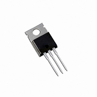
MOSFET P-CH 50V 18A TO-220AB
Manufacturer
Vishay
Series
HEXFET®r
Specifications of IRF9Z30PBF
Transistor Polarity
P-Channel
Fet Type
MOSFET P-Channel, Metal Oxide
Fet Feature
Standard
Rds On (max) @ Id, Vgs
140 mOhm @ 9.3A, 10V
Drain To Source Voltage (vdss)
50V
Current - Continuous Drain (id) @ 25° C
18A
Vgs(th) (max) @ Id
4V @ 250µA
Gate Charge (qg) @ Vgs
39nC @ 10V
Input Capacitance (ciss) @ Vds
900pF @ 25V
Power - Max
74W
Mounting Type
Through Hole
Package / Case
TO-220-3 (Straight Leads)
Minimum Operating Temperature
- 55 C
Configuration
Single
Resistance Drain-source Rds (on)
0.14 Ohm @ 10 V
Drain-source Breakdown Voltage
50 V
Gate-source Breakdown Voltage
+/- 20 V
Continuous Drain Current
18 A
Power Dissipation
74000 mW
Maximum Operating Temperature
+ 150 C
Mounting Style
Through Hole
Continuous Drain Current Id
-18A
Drain Source Voltage Vds
-50V
On Resistance Rds(on)
93mohm
Rds(on) Test Voltage Vgs
-10V
Threshold Voltage Vgs Typ
-4V
Fall Time
64 ns
Rise Time
110 ns
Lead Free Status / RoHS Status
Lead free / RoHS Compliant
Lead Free Status / RoHS Status
Lead free / RoHS Compliant, Lead free / RoHS Compliant
Other names
*IRF9Z30PBF


IRF9Z30PbF
Note:
Electrical Characteristics @ T
BV
V
I
I
I
R
g
C
C
C
t
t
t
t
Q
Q
Q
L
L
Source-Drain Diode Ratings and Characteristics
I
I
V
t
Q
T
GSS
DSS
D(on)
d(on)
r
d(off)
f
S
SM
rr
fs
D
S
GS(th)
DS(on)
iss
oss
rss
SD
on
g
gs
gd
rr
DSS
2
T
Repetitive Rating :Pulse width limited by max. junction tempeature. See Transient Thermal Impedance Curve (Fig.5).
@ V
Pulse Test : Pulse width
J
= 25°C to 150°C
dd
Drain-to-Source Breakdown Voltage
Gate Threshold Voltage
Gate-to-Source Forward Leakage
Gate-to-Source Reverse Leakage
Drain-to-Source Leakage Current
On- State Drain Current
Static Drain-to-Source On-Resistance
Forward Transconductance
Input Capacitance
Output Capacitance
Reverse Transfer Capacitance
Turn-On Delay Time
Rise Time
Turn-Off Delay Time
Fall Time
Total Gate Charge (Gate -Source Plus Gate-Drain)
Post-Vth Gate-to-Source Charge
Gate-to-Drain Charge
Internal Drain Inductance
Internal Source Inductance
Continuous Source Current
(Body Diode)
Pulsed Source Current
(Body Diode)
Diode Forward Voltage
Reverse Recovery Time
Reverse Recovery Charge
Forward Turn-on Time
= -25V, T
Parameter
J
= 25°C, L = 100µH, R
Parameter
≤
300ms, Duty Cycle
J
= 25°C (unless otherwise specified)
G
= 25Ω.
≤
2%.
Intrinsic turn-on time is negligible. Turn-on speed is substantially controlled by L
Min. Typ. Max. Units
Min. Typ. Max. Units
0.20 0.47
–––
–––
–––
–––
–––
–––
–––
–––
–––
–––
–––
–––
–––
–––
–––
–––
–––
–––
–––
–––
-2.0
3.1
54
-50
-18
0.093 0.14
–––
–––
–––
120
–––
–––
–––
–––
–––
–––
–––
900
570
140
110
4.7
6.9
9.7
4.5
7.5
12
21
64
26
-1000
250
-500
-250
–––
500
–––
–––
–––
–––
–––
170
–––
–––
-6.3
1.1
-4.0
-18
-60
18
32
96
39
10
15
µC
nC
nH
nA
µA
pF
ns
ns
Ω
A
V
V
A
S
V
Measured from the drain
Measured from the source
V
V
V
V
V
V
V
V
V
V
V
ƒ = 1.0MHz,
V
See Fig.16
(MOSFET switching times are assentially independent
of operating temperature)
VGS = -10V, ID = -18A, V
See Fig.17 for test circuit (Gate charge is essentially
independent of operating temperature.)
MOSFET symbol
showing the
integral reverse
p-n junction rectifier.
T
T
di/dt = 100A/µs
lead, 6mm (0.25 in.) from
package to center of die.
lead, 6mm (0.25 in.) from
package to source bonding pad.
GS
DS
GS
GS
DS
DS
DS
GS
DS
GS
DS
DD
J
J
= 25°C, I
= 25°C, I
> I
= 0V, I
= V
= -20V
= 20V
= Max. Rating, V
= Max. Rating x 0.8, V
= -10V, I
= 2 X V
= 0V
= -25V
= -25V, ID = -18A, RG = 13Ω, RD = 1.3Ω
D(on)
GS
, I
D
X R
D
GS
= -250µA
D
S
F
= -250µA
, I
DS(ON)
= -9.3A
= -18A, V
= -18A
DS
= -9.0A
See Fig.10
(max)., V
GS
Conditions
Conditions
= 0V
GS
GS
DS
= 0V, T
= 0V
= 0.8 Max. Rating
GS
Modified MOSFET symbol
showing
the internal
device
inductances.
= -10V
www.irf.com
J
= 125°C
S
+ L
D
.
Related parts for IRF9Z30PBF
Image
Part Number
Description
Manufacturer
Datasheet
Request
R

Part Number:
Description:
MOSFET P-CH 50V 18A TO-220AB
Manufacturer:
Vishay
Datasheet:

Part Number:
Description:
357-036-542-201 CARDEDGE 36POS DL .156 BLK LOPRO
Manufacturer:
Vishay
Datasheet:
Part Number:
Description:
357-036-542-201 CARDEDGE 36POS DL .156 BLK LOPRO
Manufacturer:
Vishay
Datasheet:
Part Number:
Description:
357-036-542-201 CARDEDGE 36POS DL .156 BLK LOPRO
Manufacturer:
Vishay
Datasheet:
Part Number:
Description:
357-036-542-201 CARDEDGE 36POS DL .156 BLK LOPRO
Manufacturer:
Vishay
Datasheet:
Part Number:
Description:
357-036-542-201 CARDEDGE 36POS DL .156 BLK LOPRO
Manufacturer:
Vishay
Datasheet:
Part Number:
Description:
357-036-542-201 CARDEDGE 36POS DL .156 BLK LOPRO
Manufacturer:
Vishay
Datasheet:
Part Number:
Description:
357-036-542-201 CARDEDGE 36POS DL .156 BLK LOPRO
Manufacturer:
Vishay
Datasheet:
Part Number:
Description:
357-036-542-201 CARDEDGE 36POS DL .156 BLK LOPRO
Manufacturer:
Vishay
Datasheet:
Part Number:
Description:
357-036-542-201 CARDEDGE 36POS DL .156 BLK LOPRO
Manufacturer:
Vishay
Datasheet:
Part Number:
Description:
357-036-542-201 CARDEDGE 36POS DL .156 BLK LOPRO
Manufacturer:
Vishay
Datasheet:
Part Number:
Description:
357-036-542-201 CARDEDGE 36POS DL .156 BLK LOPRO
Manufacturer:
Vishay
Datasheet:
Part Number:
Description:
357-036-542-201 CARDEDGE 36POS DL .156 BLK LOPRO
Manufacturer:
Vishay
Datasheet:
Part Number:
Description:
357-036-542-201 CARDEDGE 36POS DL .156 BLK LOPRO
Manufacturer:
Vishay
Datasheet:
Part Number:
Description:
357-036-542-201 CARDEDGE 36POS DL .156 BLK LOPRO
Manufacturer:
Vishay
Datasheet: