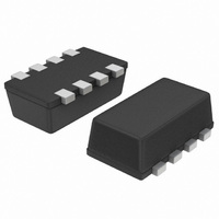
NTHS5404T1G ON Semiconductor, NTHS5404T1G Datasheet - Page 2

NTHS5404T1G
Manufacturer Part Number
NTHS5404T1G
Description
MOSFET N-CH 20V 5.2A CHIPFET
Manufacturer
ON Semiconductor
Type
Power MOSFETr
Specifications of NTHS5404T1G
Fet Type
MOSFET N-Channel, Metal Oxide
Fet Feature
Logic Level Gate
Rds On (max) @ Id, Vgs
30 mOhm @ 5.2A, 4.5V
Drain To Source Voltage (vdss)
20V
Current - Continuous Drain (id) @ 25° C
5.2A
Vgs(th) (max) @ Id
600mV @ 250µA
Gate Charge (qg) @ Vgs
18nC @ 4.5V
Power - Max
1.3W
Mounting Type
Surface Mount
Package / Case
8-ChipFET™
Number Of Elements
1
Polarity
N
Channel Mode
Enhancement
Drain-source On-res
0.03Ohm
Drain-source On-volt
20V
Gate-source Voltage (max)
±12V
Drain Current (max)
5.2A
Power Dissipation
1.3W
Output Power (max)
Not RequiredW
Frequency (max)
Not RequiredMHz
Noise Figure
Not RequireddB
Power Gain
Not RequireddB
Drain Efficiency
Not Required%
Operating Temp Range
-55C to 150C
Operating Temperature Classification
Military
Mounting
Surface Mount
Pin Count
8
Package Type
ChipFET
Configuration
Single Hex Drain
Transistor Polarity
N-Channel
Resistance Drain-source Rds (on)
0.025 Ohms
Forward Transconductance Gfs (max / Min)
20 S
Drain-source Breakdown Voltage
20 V
Gate-source Breakdown Voltage
+/- 12 V
Continuous Drain Current
7.2 A
Maximum Operating Temperature
+ 150 C
Mounting Style
SMD/SMT
Minimum Operating Temperature
- 55 C
Lead Free Status / RoHS Status
Lead free / RoHS Compliant
Other names
NTHS5404T1GOS
NTHS5404T1GOS
NTHS5404T1GOSTR
NTHS5404T1GOS
NTHS5404T1GOSTR
Available stocks
Company
Part Number
Manufacturer
Quantity
Price
Company:
Part Number:
NTHS5404T1G
Manufacturer:
ON
Quantity:
1 670
Part Number:
NTHS5404T1G
Manufacturer:
ON/安森美
Quantity:
20 000
2. Surface Mounted on FR4 board using 1 in sq pad size (Cu area = 1.127 in sq [1 oz] including traces).
3. Pulse Test: Pulse Width v 300 ms, Duty Cycle v 2%.
4. Guaranteed by design, not subject to production testing.
THERMAL CHARACTERISTICS
ELECTRICAL CHARACTERISTICS
Static
Dynamic (Note 4)
DRAIN−SOURCE DIODE CHARACTERISTICS
Gate Threshold Voltage
Gate−Body Leakage
Zero Gate Voltage Drain Current
On−State Drain Current (Note 3)
Drain−Source On−State Resistance (Note 3)
Forward Transconductance (Note 3)
Total Gate Charge
Gate−Source Charge
Gate−Drain Charge
Turn−On Delay Time
Rise Time
Turn−Off Delay Time
Fall Time
Forward Diode Voltage (Note 3)
Reverse Recovery Time
Charge Time
Discharge Time
Reverse Recovery Time
Maximum Junction−to−Ambient (Note 2)
Maximum Junction−to−Foot (Drain)
t v 5 sec
Steady State
Steady State
Characteristic
Characteristic
(T
J
= 25 C unless otherwise noted)
Symbol
V
r
I
DS(on)
t
t
I
I
Q
Q
V
GS(th)
D(on)
d(on)
d(off)
GSS
DSS
Q
g
Q
t
t
t
t
t
SD
GS
GD
rr
a
b
fs
(
r
f
G
rr
)
http://onsemi.com
NTHS5404
V
I
I
V
V
D
D
V
V
DS
V
V
V
DS
V
V
V
V
DS
DS
V
DS
^ 1 0 A V
^ 1.0 A, V
GS
GS
DS
DD
DS
GS
GS
2
GS
di
w 5.0 V, V
= 10 V, V
Test Condition
= 0 V, V
= V
= 16 V, V
S
= 16 V, V
= 4.5 V, I
= 2.5 V, I
= 10 V, R
= 10 V, I
= 0 V, I
= 0 V, I
= 0 V, I
/dt = 100 A/ms
T
I
I
Symbol
R
D
D
GS
J
R
R
G
G
= 5.2 A
= 5.2 A
= 85 C
qJA
qJF
, I
= 6 W
GS
GEN
GEN
S
S
D
GS
S
D
GS
D
D
GS
= 5.2 A,
= 5.2 A,
GS
= 250 mA
L
= 5.2 A
= "12 V
= 5.2 A
= 5.2 A
= 4.3 A
= 4.5 V,
= 10 W
= 4 5 V
= 4.5 V,
= 0 V,
= 4.5 V
= 0 V
Typ
40
80
15
Min
0.6
20
−
−
−
−
−
−
−
−
−
−
−
−
−
−
−
−
−
−
Max
0.025
0.038
20.9
10.2
10.6
Typ
50
95
20
2.4
3.2
8.0
7.0
0.8
20
12
50
28
11
−
−
−
−
−
"100
0.030
0.045
Max
1.0
5.0
1.2
18
15
15
60
40
−
−
−
−
−
−
−
−
−
Unit
C/W
C/W
Unit
nA
mA
nC
nC
ns
ns
W
V
A
S
V


