NTE4151PT1G ON Semiconductor, NTE4151PT1G Datasheet - Page 2
NTE4151PT1G
Manufacturer Part Number
NTE4151PT1G
Description
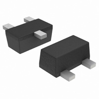
MOSFET P-CH 20V 760MA SC-89
Manufacturer
ON Semiconductor
Type
Small Signalr
Datasheet
1.NTE4151PT1G.pdf
(6 pages)
Specifications of NTE4151PT1G
Fet Type
MOSFET P-Channel, Metal Oxide
Fet Feature
Standard
Rds On (max) @ Id, Vgs
360 mOhm @ 350mA, 4.5V
Drain To Source Voltage (vdss)
20V
Current - Continuous Drain (id) @ 25° C
760mA
Vgs(th) (max) @ Id
450mV @ 250µA
Gate Charge (qg) @ Vgs
2.1nC @ 4.5V
Input Capacitance (ciss) @ Vds
156pF @ 5V
Power - Max
313mW
Mounting Type
Surface Mount
Package / Case
SC-62, SOT-89, TO-243 (3 Leads + Tab)
Configuration
Single
Transistor Polarity
P-Channel
Resistance Drain-source Rds (on)
0.36 Ohm @ 4.5 V
Forward Transconductance Gfs (max / Min)
0.4 S
Drain-source Breakdown Voltage
20 V
Gate-source Breakdown Voltage
+/- 6 V
Continuous Drain Current
0.76 A
Power Dissipation
313 mW
Maximum Operating Temperature
+ 150 C
Mounting Style
SMD/SMT
Minimum Operating Temperature
- 55 C
Number Of Elements
1
Polarity
P
Channel Mode
Enhancement
Drain-source On-res
0.36Ohm
Drain-source On-volt
20V
Gate-source Voltage (max)
±6V
Operating Temp Range
-55C to 150C
Operating Temperature Classification
Military
Mounting
Surface Mount
Pin Count
3
Package Type
SC-89
Lead Free Status / RoHS Status
Lead free / RoHS Compliant
Other names
NTE4151PT1GOSTR
Available stocks
Company
Part Number
Manufacturer
Quantity
Price
Company:

Part Number:
NTE4151PT1G
Manufacturer:
ON
Quantity:
30 000
Company:
Part Number:
NTE4151PT1G
Manufacturer:
ON
Quantity:
30 000
Company:
Part Number:
NTE4151PT1G
Manufacturer:
PANJIT
Quantity:
9 095
Part Number:
NTE4151PT1G
Manufacturer:
ON/安森美
Quantity:
20 000


2. Pulse Test: pulse width ≤ 300 ms, duty cycle ≤ 2%.
3. Switching characteristics are independent of operating junction temperatures.
†For information on tape and reel specifications, including part orientation and tape sizes, please refer to our Tape and Reel Packaging
ELECTRICAL CHARACTERISTICS
OFF CHARACTERISTICS
ON CHARACTERISTICS (Note 2)
CHARGES AND CAPACITANCES
SWITCHING CHARACTERISTICS (Note 3)
DRAIN−SOURCE DIODE CHARACTERISTICS
ORDERING INFORMATION
Specifications Brochure, BRD8011/D.
Drain−to−Source Breakdown Voltage
Zero Gate Voltage Drain Current
Gate−to−Source Leakage Current
Gate Threshold Voltage
Drain−to−Source On Resistance
Forward Transconductance
Input Capacitance
Output Capacitance
Reverse Transfer Capacitance
Total Gate Charge
Threshold Gate Charge
Gate−to−Source Charge
Gate−to−Drain Charge
Turn−On Delay Time
Rise Time
Turn−Off Delay Time
Fall Time
Forward Diode Voltage
NTA4151PT1
NTA4151PT1G
NTE4151PT1G
Parameter
Device
(T
J
V
= 25°C unless otherwise stated)
Symbol
V
Q
R
Q
td
Marking
(BR)DSS
td
C
C
GS(TH)
I
I
C
G(TOT)
Q
Q
DS(on)
V
g
DSS
GSS
G(TH)
(OFF)
OSS
RSS
(ON)
FS
ISS
t
t
TN
TN
TM
GS
GD
SD
r
f
NTA4151P, NTE4151P
http://onsemi.com
V
V
V
V
V
V
I
V
GS
GS
GS
GS
GS
V
V
V
V
DS
D
V
DS
GS
DS
GS
GS
GS
= −200 mA, R
= −4.5 V, V
= −4.5 V, I
= −2.5 V, I
= −1.8 V, I
= −4.5 V, V
= −10 V, I
Test Condition
= V
2
= 0 V, V
= 0 V, I
= 0 V, f = 1.0 MHz,
(Pb−Free)
(Pb−Free)
= 0 V, I
= 0 V, V
Package
V
SC−75
SC−75
SC−89
I
DS
D
GS
= −0.3 A
= −5.0 V
, I
S
D
D
GS
D
DS
D
D
D
= −250 mA
= −250 mA
DD
DD
= −250 mA
= −250 mA
= −350 mA
= −300 mA
= −150 mA
= ±4.5 V
G
= −16 V
= −10 V,
= −10 V,
= 10 W
−0.45
Min
−20
3000/Tape & Reel
3000/Tape & Reel
3000/Tape & Reel
Shipping
0.125
0.325
−0.72
$1.0
−1.0
0.26
0.35
0.49
20.4
Typ
156
0.4
2.1
0.5
8.0
8.2
28
18
29
†
−100
$10
Max
0.36
0.45
−1.1
1.0
Unit
nA
mA
nC
pF
ns
W
V
V
S
V
Related parts for NTE4151PT1G
Image
Part Number
Description
Manufacturer
Datasheet
Request
R

Part Number:
Description:
TRANSFORMER, AUDIO, 1:4
Manufacturer:
Neutrik
Datasheet:

Part Number:
Description:
ON Semiconductor [VOLTAGE REGULATOR]
Manufacturer:
ON Semiconductor
Datasheet:
Part Number:
Description:
357-036-542-201 CARDEDGE 36POS DL .156 BLK LOPRO
Manufacturer:
ON Semiconductor
Datasheet:
Part Number:
Description:
357-036-542-201 CARDEDGE 36POS DL .156 BLK LOPRO
Manufacturer:
ON Semiconductor
Datasheet:
Part Number:
Description:
357-036-542-201 CARDEDGE 36POS DL .156 BLK LOPRO
Manufacturer:
ON Semiconductor
Datasheet:
Part Number:
Description:
357-036-542-201 CARDEDGE 36POS DL .156 BLK LOPRO
Manufacturer:
ON Semiconductor
Datasheet:
Part Number:
Description:
357-036-542-201 CARDEDGE 36POS DL .156 BLK LOPRO
Manufacturer:
ON Semiconductor
Datasheet:
Part Number:
Description:
357-036-542-201 CARDEDGE 36POS DL .156 BLK LOPRO
Manufacturer:
ON Semiconductor
Datasheet:
Part Number:
Description:
357-036-542-201 CARDEDGE 36POS DL .156 BLK LOPRO
Manufacturer:
ON Semiconductor
Datasheet:
Part Number:
Description:
357-036-542-201 CARDEDGE 36POS DL .156 BLK LOPRO
Manufacturer:
ON Semiconductor
Datasheet:
Part Number:
Description:
357-036-542-201 CARDEDGE 36POS DL .156 BLK LOPRO
Manufacturer:
ON Semiconductor
Datasheet:
Part Number:
Description:
357-036-542-201 CARDEDGE 36POS DL .156 BLK LOPRO
Manufacturer:
ON Semiconductor
Datasheet:
Part Number:
Description:
Manufacturer:
ON Semiconductor
Datasheet:
Part Number:
Description:
Manufacturer:
ON Semiconductor
Datasheet: