STV160NF03LT4 STMicroelectronics, STV160NF03LT4 Datasheet

MOSFET N-CH 30V 160A POWERSO-10

STV160NF03LT4

Manufacturer Part Number
STV160NF03LT4
Description
MOSFET N-CH 30V 160A POWERSO-10
Manufacturer
STMicroelectronics
Series
STripFET™r
Datasheet

Specifications of STV160NF03LT4

Fet Type
MOSFET N-Channel, Metal Oxide
Fet Feature
Logic Level Gate
Rds On (max) @ Id, Vgs
2.8 mOhm @ 80A, 10V
Drain To Source Voltage (vdss)
30V
Current - Continuous Drain (id) @ 25° C
160A
Vgs(th) (max) @ Id
1V @ 250µA
Gate Charge (qg) @ Vgs
140nC @ 10V
Input Capacitance (ciss) @ Vds
4700pF @ 25V
Power - Max
210W
Mounting Type
Surface Mount
Package / Case
PowerSO-10 Exposed Bottom Pad
Configuration
Single
Transistor Polarity
N-Channel
Resistance Drain-source Rds (on)
0.0019 Ohms
Forward Transconductance Gfs (max / Min)
210 S
Drain-source Breakdown Voltage
30 V
Gate-source Breakdown Voltage
+/- 15 V
Continuous Drain Current
160 A
Power Dissipation
210 W
Maximum Operating Temperature
+ 175 C
Mounting Style
SMD/SMT
Minimum Operating Temperature
- 65 C
Lead Free Status / RoHS Status
Lead free / RoHS Compliant
Other names
497-3252-2

Available stocks

Company
Part Number
Manufacturer
Quantity
Price
Part Number:
STV160NF03LT4
Manufacturer:
ST
0
Part Number:
STV160NF03LT4
Manufacturer:
ST
Quantity:
20 000
DESCRIPTION
The STV160NF03L represents the second gener-
ation of Application Specific STMicroelectronics
well established STripFET™ process based on a
very unique strip layout design. The resulting
MOSFET shows unrivalled high packing density
with ultra low on-resistance and superior switching
charactestics. Process simplification also trans-
lates into improved manufacturing reproducibility.
This device is particularly suitable for high current,
low voltage switching application where efficiency
is crucial
APPLICATIONS
ABSOLUTE MAXIMUM RATINGS
( ) Pulse width limited by safe operating area
November 2002
STV160NF03L
TYPICAL R
LOW THRESHOLD DRIVE
ULTRA LOW ON-RESISTANCE
ULTRA FAST SWITCHING
100% AVALANCHE TESTED
VERY LOW GATE CHARGE
LOW PROFILE, VERY LOW PARASITIC
INDUCTANCE PowerSO-10 PACKAGE
BUCK CONVERTERS IN HIGH
PERFORMANCE TELECOM AND VRMs DC-
DC CONVERTERS
Symbol
E
I
V
I
DM
P
V
AS
V
D
T
DGR
TOT
I
T
(**)
stg
DS
GS
TYPE
D
j
( )
(1)
Drain-source Voltage (V
Drain-gate Voltage (R
Gate- source Voltage
Drain Current (continuos) at T
Drain Current (pulsed)
Total Dissipation at T
Derating Factor
Single Pulse Avalanche Energy
Storage Temperature
Max. Operating Junction Temperature
DS
(on) = 0.0019
V
30 V
DSS
N-CHANNEL 30V - 0.0019 - 160A PowerSO-10
< 0.0028
R
DS(on)
C
GS
Parameter
= 25°C
GS
= 20 k )
= 0)
C
C
= 25°C
= 100°C
160 A
I
D
STripFET™ POWER MOSFET
(1) Starting T
(**)Limited only maximum junction temperature allowed by
PowerSO-10
CONNECTION DIAGRAM (TOP VIEW)
INTERNAL SCHEMATIC DIAGRAM
j
=25°C , I
D
10
PowerSO-10
= 80A, V
STV160NF03L
–65 to 175
Value
± 15
160
640
210
175
113
1.4
30
30
1
DD
= 20V
1
W/°C
Unit
°C
°C
W
V
V
V
A
A
A
J
1/9

Related parts for STV160NF03LT4

STV160NF03LT4 Summary of contents

Page 1

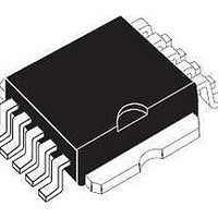
... LOW PROFILE, VERY LOW PARASITIC INDUCTANCE PowerSO-10 PACKAGE DESCRIPTION The STV160NF03L represents the second gener- ation of Application Specific STMicroelectronics well established STripFET™ process based on a very unique strip layout design. The resulting MOSFET shows unrivalled high packing density with ultra low on-resistance and superior switching charactestics ...

Page 2

STV160NF03L THERMAL DATA Rthj-case Thermal Resistance Junction-case Max Rthj-amb Thermal Resistance Junction-ambient Max T Maximum Lead Temperature For Soldering Purpose l ELECTRICAL CHARACTERISTICS (TCASE = 25 °C UNLESS OTHERWISE SPECIFIED) OFF Symbol Parameter V Drain-source (BR)DSS Breakdown Voltage I Zero ...

Page 3

ELECTRICAL CHARACTERISTICS (CONTINUED) SWITCHING ON Symbol Parameter t Turn-on Delay Time d(on) t Rise Time r Q Total Gate Charge g Q Gate-Source Charge gs Q Gate-Drain Charge gd SWITCHING OFF Symbol Parameter t Turn-off-Delay Time d(off) Fall Time t ...

Page 4

STV160NF03L Output Characteristics Tranconductance Gate Charge vs Gate-source Voltage 4/9 Tranfer Characteristics Static Drain-Source On Resistance Capacitance Variations ...

Page 5

Normalized Gate Thereshold Voltage vs Temp. Source-drain Diode Forward Characteristics Basic Schematic For Motherboard VRM Whith Synchronous Rectification Normalized On Resistance vs Temperature Basic Schematic Mosfets Switch Used In Secondary Side Of a Froward Convert STV160NF03L 5/9 ...

Page 6

STV160NF03L 6/9 ...

Page 7

Fig. 1: Unclamped Inductive Load Test Circuit Fig. 3: Switching Times Test Circuit For Resistive Load Fig. 5: Test Circuit For Inductive Load Switching And Diode Recovery Times Fig. 2: Unclamped Inductive Waveform Fig. 4: Gate Charge test Circuit STV160NF03L ...

Page 8

STV160NF03L DIM. MIN. A 3.35 A1 0.00 B 0.40 C 0.35 D 9. 9.30 E1 7.20 E2 7.20 E3 6.10 E4 5. 13. ...

Page 9

... No license is granted by implication or otherwise under any patent or patent rights of STMicroelectronics. Specifications mentioned in this publication are subject to change without notice. This publication supersedes and replaces all information previously supplied ...

Related keywords