IXFA10N60P IXYS, IXFA10N60P Datasheet - Page 2
IXFA10N60P
Manufacturer Part Number
IXFA10N60P
Description
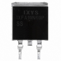
MOSFET N-CH 600V 10A D2-PAK
Manufacturer
IXYS
Series
PolarHV™r
Datasheet
1.IXFA10N60P.pdf
(4 pages)
Specifications of IXFA10N60P
Fet Type
MOSFET N-Channel, Metal Oxide
Fet Feature
Standard
Rds On (max) @ Id, Vgs
740 mOhm @ 500mA, 10V
Drain To Source Voltage (vdss)
600V
Current - Continuous Drain (id) @ 25° C
10A
Vgs(th) (max) @ Id
5.5V @ 1mA
Gate Charge (qg) @ Vgs
32nC @ 10V
Input Capacitance (ciss) @ Vds
1610pF @ 25V
Power - Max
200W
Mounting Type
Surface Mount
Package / Case
D²Pak, TO-263 (2 leads + tab)
Configuration
Single
Transistor Polarity
N-Channel
Resistance Drain-source Rds (on)
0.74 Ohm @ 10 V
Forward Transconductance Gfs (max / Min)
11 s
Drain-source Breakdown Voltage
600 V
Gate-source Breakdown Voltage
+/- 30 V
Continuous Drain Current
10 A
Power Dissipation
200000 mW
Maximum Operating Temperature
+ 150 C
Mounting Style
SMD/SMT
Minimum Operating Temperature
- 55 C
Vdss, Max, (v)
600
Id(cont), Tc=25°c, (a)
10
Rds(on), Max, Tj=25°c, (?)
0.74
Ciss, Typ, (pf)
1720
Qg, Typ, (nc)
32
Trr, Typ, (ns)
120
Trr, Max, (ns)
200
Pd, (w)
200
Rthjc, Max, (ºc/w)
0.62
Package Style
TO-263
Lead Free Status / RoHS Status
Lead free / RoHS Compliant
Available stocks
Company
Part Number
Manufacturer
Quantity
Price
Company:

Part Number:
IXFA10N60P
Manufacturer:
IXYS
Quantity:
18 000


Notes: 1.
IXYS MOSFETs and IGBTs are covered
by one or more of the following U.S. patents: 4,850,072
Symbol
(T
g
C
C
C
t
t
t
t
Q
Q
Q
R
R
Source-Drain Diode
Symbol
(T
I
I
V
t
I
Q
S
SM
RM
d(on)
r
d(off)
f
rr
IXYS Reserves the Right to Change Limits, Test Conditions, and Dimensions.
fs
SD
iss
oss
rss
thJC
thCH
g(on)
gs
gd
RM
J
J
= 25°C, Unless Otherwise Specified)
= 25°C, Unless Otherwise Specified)
2. On through-hole packages, R
location must be 5mm or less from the package body.
Pulse test, t ≤ 300μs, duty cycle, d ≤ 2%.
V
Repetitive, Pulse Width Limited by T
V
Resistive Switching Times
V
R
V
V
I
I
-di/dt = 100A/μs
V
Test Conditions
TO-220
Test Conditions
F
F
DS
GS
GS
GS
R
GS
G
= 0.5 • I
= I
= 100V
= 10V, I
= 10Ω (External)
= 0V, V
= 10V, V
= 0V
= 10V, V
S
, V
GS
D25
= 0V, Note 1
DS
D
, V
DS
DS
= 0.5 • I
= 25V, f = 1MHz
GS
= 0.5 • V
= 0.5 • V
4,835,592
4,881,106
= 0V
D25
, Note 1
DSS
DSS
4,931,844
5,017,508
5,034,796
, I
, I
DS(on)
D
D
= 0.5 • I
= 0.5 • I
Kelvin test contact
5,049,961
5,063,307
5,187,117
JM
D25
D25
5,237,481
5,381,025
5,486,715
Min.
Min.
Characteristic Values
Characteristic Values
6
6,162,665
6,259,123 B1
6,306,728 B1
1720
Typ.
Typ.
0.50
320
160
120
65
14
32
12
10
11
27
21
23
3
Max.
Max.
0.62 °C/W
200
1.5
10
6,404,065 B1
6,534,343
6,583,505
30
°C/W
nC
nC
nC
nC
pF
pF
pF
ns
ns
ns
ns
ns
S
A
A
V
A
6,683,344
6,710,405 B2 6,759,692
6,710,463
TO-263 Outline
TO-220 Outline
Pins: 1 - Gate
6,727,585
6,771,478 B2 7,071,537
3 - Source
7,005,734 B2
7,063,975 B2
IXFA10N60P
IXFP10N60P
2 - Drain
7,157,338B2
Related parts for IXFA10N60P
Image
Part Number
Description
Manufacturer
Datasheet
Request
R

Part Number:
Description:
TRANS MOSFET N-CH 1200V 3A 3TO-263
Manufacturer:
IXYS Corporation
Datasheet:

Part Number:
Description:
HiPerFET Power MOSFETs
Manufacturer:
IXYS Corporation
Datasheet:
Part Number:
Description:
J-K-Type Flip-Flop
Manufacturer:
IXYS Corporation
Datasheet:
Part Number:
Description:
HiPerRF Power MOSFETs
Manufacturer:
IXYS Corporation
Datasheet:
Part Number:
Description:
Rectifier Module for Three Phase Power Factor Correction
Manufacturer:
IXYS Corporation
Datasheet:
Part Number:
Description:
Thyristor Modules Thyristor/Diode Modules
Manufacturer:
IXYS Corporation
Datasheet:
Part Number:
Description:
Thyristor Modules Thyristor/Diode Modules
Manufacturer:
IXYS Corporation
Datasheet:
Part Number:
Description:
Thyristor Modules Thyristor/Diode Modules
Manufacturer:
IXYS Corporation
Datasheet:
Part Number:
Description:
Thyristor Modules Thyristor/Diode Modules
Manufacturer:
IXYS Corporation
Datasheet:
Part Number:
Description:
Thyristor Modules /Diode Modules
Manufacturer:
IXYS Corporation
Datasheet:
Part Number:
Description:
Thyristor Modules /Diode Modules
Manufacturer:
IXYS Corporation
Datasheet: