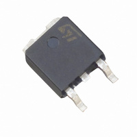
STD95NH02LT4 STMicroelectronics, STD95NH02LT4 Datasheet

STD95NH02LT4
Specifications of STD95NH02LT4
Related parts for STD95NH02LT4
STD95NH02LT4 Summary of contents
Page 1
... DC- DC converters. It’s therefore ideal for high-density converters in Telecom and Computer applications. Application ■ Switching applications Table 1. Device summary Order code STD95NH02LT4 STD95NH02L-1 August 2007 N-channel 24V - 0.0039Ω - 80A - DPAK - IPAK R I DS(on) D (1) < 0.005Ω 80A (1) < ...
Page 2
Contents Contents 1 Electrical ratings . . . . . . . . . . . . . . . . . . . . . . . . . . . . . . . . . . . ...
Page 3
STD95NH02L - STD95NH02L-1 1 Electrical ratings Table 2. Absolute maximum ratings Symbol (1) V Drain-source voltage rating spike V Drain-source voltage ( Drain-gate voltage (R DGR V Gate-source voltage GS (2) I Drain current (continuous ...
Page 4
Electrical characteristics 2 Electrical characteristics (T =25°C unless otherwise specified) CASE Table 4. On/off states Symbol Drain-source V (BR)DSS breakdown voltage Zero gate voltage I DSS drain current (V Gate-body leakage I GSS current (V V Gate threshold voltage GS(th) ...
Page 5
STD95NH02L - STD95NH02L-1 Table 6. Source drain diode Symbol Source-drain current I SD Source-drain current (1) I SDM (pulsed) (2) V Forward on voltage SD t Reverse recovery time rr Q Reverse recovery charge rr I Reverse recovery current RRM ...
Page 6
Electrical characteristics 2.1 Electrical characteristics (curves) Figure 2. Safe operating area Figure 4. Output characteristics Figure 6. Transconductance 6/16 STD95NH02L - STD95NH02L-1 Figure 3. Thermal impedance Figure 5. Transfer characteristics Figure 7. Static drain-source on resistance ...
Page 7
STD95NH02L - STD95NH02L-1 Figure 8. Gate charge vs gate-source voltage Figure 9. Figure 10. Normalized gate threshold voltage vs temperature Figure 12. Source-drain diode forward characteristics Electrical characteristics Capacitance variations Figure 11. Normalized on resistance vs temperature Figure 13. Normalized ...
Page 8
Test circuit 3 Test circuit Figure 14. Switching times test circuit for resistive load Figure 16. Test circuit for inductive load switching and diode recovery times Figure 18. Unclamped inductive waveform 8/16 STD95NH02L - STD95NH02L-1 Figure 15. Gate charge test ...
Page 9
STD95NH02L - STD95NH02L-1 4 Appendix A Figure 20. Buck converter: power losses estimation The power losses associated with the FETs in a synchronous buck converter can be estimated using the equations shown in the table below. The formulas give a ...
Page 10
Appendix A Table 7. Power losses calculation Recovery (1) Pdiode Conductio n Pgate Qoss 1. Dissipated by SW1 during turn-on Table 8. Parameters meaning Parameter d Q gsth Q gls Pconduction Pswitching Pdiode Pgate P Qoss 10/16 ...
Page 11
STD95NH02L - STD95NH02L-1 5 Package mechanical data In order to meet environmental requirements, ST offers these devices in ECOPACK® packages. These packages have a Lead-free second level interconnect. The category of second level interconnect is marked on the package and ...
Page 12
Package mechanical data DIM (L1 12/16 DPAK MECHANICAL DATA mm. MIN. TYP MAX. 2.2 2.4 0.9 1.1 0.03 0.23 0.64 0.9 ...
Page 13
STD95NH02L - STD95NH02L-1 DIM TO-251 (IPAK) MECHANICAL DATA mm MIN. TYP. MAX. 2.2 2.4 0.9 1.1 0.7 1.3 0.64 0.9 5.2 5.4 0.85 ...
Page 14
Packing mechanical data 6 Packing mechanical data DPAK FOOTPRINT All dimensions are in millimeters TAPE MECHANICAL DATA mm DIM. MIN. A0 6 1.5 D1 1.5 E 1.65 F 7.4 K0 2.55 P0 3.9 P1 7.9 P2 ...
Page 15
STD95NH02L - STD95NH02L-1 7 Revision history Table 9. Revision history Date 13-Sep-2004 27-May-2005 09-Aug-2006 02-Aug-2007 Revision 1 First release 2 Some values changed in 3 The document has been updated 4 Error on cover page; added IPAK Revision history Changes ...
Page 16
... Information in this document is provided solely in connection with ST products. STMicroelectronics NV and its subsidiaries (“ST”) reserve the right to make changes, corrections, modifications or improvements, to this document, and the products and services described herein at any time, without notice. All ST products are sold pursuant to ST’s terms and conditions of sale. ...


