STP12PF06 STMicroelectronics, STP12PF06 Datasheet

MOSFET P-CH 60V 12A TO-220

STP12PF06

Manufacturer Part Number
STP12PF06
Description
MOSFET P-CH 60V 12A TO-220
Manufacturer
STMicroelectronics
Series
STripFET™r
Datasheet

Specifications of STP12PF06

Fet Type
MOSFET P-Channel, Metal Oxide
Fet Feature
Standard
Rds On (max) @ Id, Vgs
200 mOhm @ 10A, 10V
Drain To Source Voltage (vdss)
60V
Current - Continuous Drain (id) @ 25° C
12A
Vgs(th) (max) @ Id
4V @ 250µA
Gate Charge (qg) @ Vgs
21nC @ 10V
Input Capacitance (ciss) @ Vds
850pF @ 25V
Power - Max
60W
Mounting Type
Through Hole
Package / Case
TO-220-3 (Straight Leads)
Configuration
Single
Transistor Polarity
P-Channel
Resistance Drain-source Rds (on)
0.2 Ohm @ 10 V
Forward Transconductance Gfs (max / Min)
6 S
Drain-source Breakdown Voltage
60 V
Gate-source Breakdown Voltage
+/- 20 V
Continuous Drain Current
12 A
Power Dissipation
60000 mW
Maximum Operating Temperature
+ 175 C
Mounting Style
Through Hole
Minimum Operating Temperature
- 55 C
Lead Free Status / RoHS Status
Lead free / RoHS Compliant
Other names
497-2721-5

Available stocks

Company
Part Number
Manufacturer
Quantity
Price
Part Number:
STP12PF06
Manufacturer:
AXELITE
Quantity:
12 000
Part Number:
STP12PF06
Quantity:
4 000
Part Number:
STP12PF06
Manufacturer:
STMicroelectronics
Quantity:
38 746
Part Number:
STP12PF06
Manufacturer:
ST
0
Company:
Part Number:
STP12PF06
Quantity:
30 800
Part Number:
STP12PF06,12PF06
Manufacturer:
ST
0
Part Number:
STP12PF06,P12PF06
Manufacturer:
ST
0
Part Number:
STP12PF06������
Manufacturer:
ST
0
Table 1: General Features
DESCRIPTION
This Power MOSFET is the latest development of
STMicroelectronis unique "Single Feature Size™"
strip-based process. The resulting transistor
shows extremely high packing density for low on-
resistance, rugged avalanche characteristics and
less
remarkable manufacturing reproducibility
APPLICATIONS
Table 2: Order Codes
Table 3: ABSOLUTE MAXIMUM RATINGS
(
NOTE
and current has to be reversed.
March 2005
STP12PF06
STF12PF06
STP12PF06
STF12PF06
TYPICAL R
EXCEPTIONAL dv/dt CAPABILITY
100% AVALANCHE TESTED
LOW GATE CHARGE
APPLICATION ORIENTED
CHARACTERIZATION
MOTOR CONTROL
DC-DC & DC-AC CONVERTERS
Pulse width limited by safe operating area.
Symbol
dv/dt
E
I
V
DM
V
:
V
AS (2)
T
P
For the P-CHANNEL MOSFET actual polarity of voltages
DGR
I
I
T
GS
stg
DS
TYPE
D
D
tot
critical
PART NUMBER
(
j
(1)
Drain-source Voltage (V
Drain-gate Voltage (R
Gate- source Voltage
Drain Current (continuous) at T
Drain Current (pulsed)
Total Dissipation at T
Derating Factor
Peak Diode Recovery voltage slope
Single Pulse Avalanche Energy
Storage Temperature
Operating Junction Temperature
DS
alignment
(on) = 0.18
P-CHANNEL 60V - 0.18
V
60 V
60 V
DSS
Parameter
steps
< 0.20
< 0.20
R
DS(on)
C
GS
= 25°C
GS
= 20 k )
therefore
MARKING
= 0)
P12PF06
F12PF06
C
C
12 A
12 A
= 25°C
= 100°C
I
D
a
STripFET™ II POWER MOSFET
Figure 1: Package
Figure 2: Internal Schematic Diagram
(1) I
(2) Starting T
STP20PF06
SD
8.4
0.4
12
48
60
12A, di/dt 200A/µs, V
PACKAGE
TO-220FP
- 12A TO-220/TO-220FP
TO-220
j
TO-220
= 25
-55 to 175
o
Value
C, I
± 20
200
Rev.
60
60
6
1
D
= 12A, V
2
3
2.0
STF20PF06
DD
STP12PF06
STF12PF06
DD
0.17
225
5.6
32
V
8
= 25V
(BR)DSS
PACKAGING
TO-220FP
, T
TUBE
TUBE
j
T
JMAX
1
2
W/°C
V/ns
Unit
mJ
°C
W
3
V
V
V
A
A
A
1/10

Related parts for STP12PF06

STP12PF06 Summary of contents

Page 1

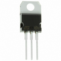
... Figure 1: Package R I DS(on) D < 0. < 0. Figure 2: Internal Schematic Diagram therefore a MARKING P12PF06 F12PF06 STP20PF06 = 25° 100° 25° (2) Starting T STP12PF06 STF12PF06 - 12A TO-220/TO-220FP TO-220 TO-220FP PACKAGE PACKAGING TO-220 TUBE TO-220FP TUBE Value STF20PF06 60 60 ± 8.4 5 225 0.4 0.17 ...

Page 2

... STP12PF06 STF12PF06 Table 4: THERMAL DATA Rthj-case Thermal Resistance Junction-case Rthj-amb Thermal Resistance Junction-ambient T Maximum Lead Temperature For Soldering Purpose l ELECTRICAL CHARACTERISTICS (T Table 5: OFF Symbol Parameter Drain-source V (BR)DSS Breakdown Voltage Zero Gate Voltage I DSS Drain Current (V GS Gate-body Leakage I GSS Current ( (*) ...

Page 3

... STP12PF06 STF12PF06 ELECTRICAL CHARACTERISTICS (continued) Table 8: SWITCHING ON Symbol Parameter t Turn-on Delay Time d(on) Rise Time Total Gate Charge g Q Gate-Source Charge gs Q Gate-Drain Charge gd Table 9: SWITCHING OFF Symbol Parameter Turn-off Delay Time t d(off) Fall Time t f Table 10: SOURCE DRAIN DIODE Symbol ...

Page 4

... STP12PF06 STF12PF06 Figure 5: Thermal Impedance Figure 7: Output Characteristics Figure 9: Transconductance 4/10 Figure 6: Thermal Impedance for TO-220FP Figure 8: Transfer Characteristics Figure 10: Static Drain-source On Resistance ...

Page 5

... STP12PF06 STF12PF06 Figure 11: Gate Charge vs Gate-source Voltage Figure 13: Normalized Gate Threshold Voltage vs Temperature Figure 15: Source-drain Diode Forward Characteristics Figure 12: Capacitance Variations Figure 14: Normalized on Resistance vs Temperature Figure 16: Normalized Breakdown Voltage Temperature 5/10 ...

Page 6

... STP12PF06 STF12PF06 Unclamped Inductive Load Test Circuit Figure 17: Switching Times Test Circuits For Re- Figure 19: sistive Load Test Circuit For Inductive Load Figure 21: Switching And Diode Recovery Times 6/10 Unclamped Inductive Waveform Figure 18: Gate Charge test Circuit Figure 20: ...

Page 7

... STP12PF06 STF12PF06 DIM. MIN. A 4.4 C 1.23 D 2.40 E 0.49 F 0.61 F1 1.14 F2 1.14 G 4. 2.65 L6 15.25 L7 6.20 L9 3.50 DIA 3.75 TO-220 MECHANICAL DATA mm. TYP. MAX. 4.6 0.173 1.32 0.048 2.72 0.094 0.70 0.019 0.88 0.024 1.70 0.044 1.70 0.044 5.15 0.194 2.70 ...

Page 8

... STP12PF06 STF12PF06 DIM. MIN. A 4.4 B 2.5 D 2.5 E 0.45 F 0.75 F1 1.15 F2 1.15 G 4. 28.6 L4 9 Ø 3 ¯ 8/10 TO-220FP MECHANICAL DATA mm TYP. MAX. 4.6 2.7 2.75 0.7 1 1.7 1.7 5.2 2.7 10.4 16 30.6 10.6 16.4 9.3 3 inch MIN. TYP. MAX. ...

Page 9

... STP12PF06 STF12PF06 Table 11: Revision History Date Revision March 2005 1.0 March 2005 2.0 Description of Changes FIRST ISSUE MINOR REVISION 9/10 ...

Page 10

... STP12PF06 STF12PF06 Information furnished is believed to be accurate and reliable. However, STMicroelectronics assumes no responsibility for the consequences of use of such information nor for any infringement of patents or other rights of third parties which may result from its use. No license is granted by implication or otherwise under any patent or patent rights of STMicroelectronics. Specifications mentioned in this publication are subject to change without notice ...

Related keywords