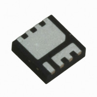
IRFH3707TR2PBF International Rectifier, IRFH3707TR2PBF Datasheet - Page 4

IRFH3707TR2PBF
Manufacturer Part Number
IRFH3707TR2PBF
Description
MOSFET N-CH 30V 12A PQFN33
Manufacturer
International Rectifier
Series
HEXFET®r
Datasheet
1.IRFH3707TR2PBF.pdf
(10 pages)
Specifications of IRFH3707TR2PBF
Fet Type
MOSFET N-Channel, Metal Oxide
Fet Feature
Logic Level Gate
Rds On (max) @ Id, Vgs
12.4 mOhm @ 12A, 10V
Drain To Source Voltage (vdss)
30V
Current - Continuous Drain (id) @ 25° C
12A
Vgs(th) (max) @ Id
2.35V @ 25µA
Gate Charge (qg) @ Vgs
8.1nC @ 4.5V
Input Capacitance (ciss) @ Vds
755pF @ 15V
Power - Max
2.8W
Mounting Type
Surface Mount
Package / Case
8-PQFN, 8-PowerQFN
Transistor Polarity
N Channel
Drain Source Voltage Vds
30V
On Resistance Rds(on)
9.4mohm
Rds(on) Test Voltage Vgs
10V
Operating Temperature Range
-55°C To +150°C
Transistor Case Style
PQFN
Rohs Compliant
Yes
Resistance Drain-source Rds (on)
17.9 mOhms
Drain-source Breakdown Voltage
30 V
Gate-source Breakdown Voltage
20 V
Continuous Drain Current
29 A
Power Dissipation
2.8 W
Gate Charge Qg
5.4 nC
Lead Free Status / RoHS Status
Lead free / RoHS Compliant
Other names
IRFH3707TR2PBFTR
4
10000
1000
1000
100
100
0.1
10
10
1
Fig 5. Typical Capacitance Vs.
Fig 7. Typical Source-Drain Diode
0.2
1
Drain-to-Source Voltage
T
0.4
J
V SD , Source-to-Drain Voltage (V)
V DS , Drain-to-Source Voltage (V)
= 150°C
V GS = 0V,
C iss = C gs + C gd , C ds SHORTED
C rss = C gd
C oss = C ds + C gd
Forward Voltage
0.6
C rss
C oss
0.8
C iss
T J = 25°C
f = 1 MHZ
10
1
V GS = 0V
1.2
1.4
1.6
100
1000
14.0
12.0
10.0
100
0.1
8.0
6.0
4.0
2.0
0.0
10
1
Fig 8. Maximum Safe Operating Area
0
0
Fig 6. Typical Gate Charge Vs.
T A = 25°C
Tj = 150°C
Single Pulse
I D = 9.4A
Gate-to-Source Voltage
2
V DS , Drain-to-Source Voltage (V)
Q G , Total Gate Charge (nC)
4
OPERATION IN THIS AREA
LIMITED BY R DS (on)
1
6
V DS = 24V
V DS = 15V
8
100µsec
10msec
10
www.irf.com
10
1msec
12
14
100
16


