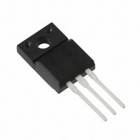
IRFI9540GPBF Vishay, IRFI9540GPBF Datasheet - Page 5

IRFI9540GPBF
Manufacturer Part Number
IRFI9540GPBF
Description
MOSFET P-CH 100V 11A TO220FP
Manufacturer
Vishay
Specifications of IRFI9540GPBF
Transistor Polarity
P-Channel
Fet Type
MOSFET P-Channel, Metal Oxide
Fet Feature
Standard
Rds On (max) @ Id, Vgs
200 mOhm @ 6.6A, 10V
Drain To Source Voltage (vdss)
100V
Current - Continuous Drain (id) @ 25° C
11A
Vgs(th) (max) @ Id
4V @ 250µA
Gate Charge (qg) @ Vgs
61nC @ 10V
Input Capacitance (ciss) @ Vds
1400pF @ 25V
Power - Max
48W
Mounting Type
Through Hole
Package / Case
TO-220-3 Full Pack (Straight Leads, Isolated), ITO-220AB
Minimum Operating Temperature
- 55 C
Configuration
Single
Resistance Drain-source Rds (on)
0.2 Ohm @ 10 V
Drain-source Breakdown Voltage
100 V
Gate-source Breakdown Voltage
+/- 20 V
Continuous Drain Current
11 A
Power Dissipation
48000 mW
Maximum Operating Temperature
+ 175 C
Mounting Style
Through Hole
Continuous Drain Current Id
-11A
Drain Source Voltage Vds
-100V
On Resistance Rds(on)
200mohm
Rds(on) Test Voltage Vgs
-10V
Threshold Voltage Vgs Typ
-4V
Fall Time
86 ns
Rise Time
110 ns
Lead Free Status / RoHS Status
Lead free / RoHS Compliant
Lead Free Status / RoHS Status
Lead free / RoHS Compliant, Lead free / RoHS Compliant
Other names
*IRFI9540GPBF
Document Number: 91164
S09-0011-Rev. A, 19-Jan-09
Vary t
required I
Fig. 9 - Maximum Drain Current vs. Case Temperature
p
Fig. 12a - Unclamped Inductive Test Circuit
to obtain
AS
R
- 10 V
G
V
DS
t
p
Fig. 11 - Maximum Effective Transient Thermal Impedance, Junction-to-Case
I
AS
D.U.T.
0.01 Ω
L
+
-
V
DD
Fig. 12b - Unclamped Inductive Waveforms
V
10 %
90 %
I
Fig. 10a - Switching Time Test Circuit
Fig. 10b - Switching Time Waveforms
AS
DS
V
V
GS
DS
R
IRFI9540G, SiHFI9540G
Pulse width ≤ 1 µs
Duty factor ≤ 0.1 %
G
- 10 V
V
t
GS
d(on)
V
DS
t
r
t
p
D.U.T.
R
Vishay Siliconix
D
t
d(off)
V
DS
t
f
+
-
www.vishay.com
V
V
DD
DD
5


