IRF644SPBF Vishay, IRF644SPBF Datasheet - Page 3
IRF644SPBF
Manufacturer Part Number
IRF644SPBF
Description
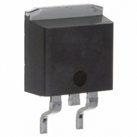
MOSFET N-CH 250V 14A D2PAK
Manufacturer
Vishay
Specifications of IRF644SPBF
Transistor Polarity
N-Channel
Fet Type
MOSFET N-Channel, Metal Oxide
Fet Feature
Standard
Rds On (max) @ Id, Vgs
280 mOhm @ 8.4A, 10V
Drain To Source Voltage (vdss)
250V
Current - Continuous Drain (id) @ 25° C
14A
Vgs(th) (max) @ Id
4V @ 250µA
Gate Charge (qg) @ Vgs
68nC @ 10V
Input Capacitance (ciss) @ Vds
1300pF @ 25V
Power - Max
3.1W
Mounting Type
Surface Mount
Package / Case
D²Pak, TO-263 (2 leads + tab)
Minimum Operating Temperature
- 55 C
Configuration
Single
Resistance Drain-source Rds (on)
0.28 Ohm @ 10 V
Drain-source Breakdown Voltage
250 V
Gate-source Breakdown Voltage
+/- 20 V
Continuous Drain Current
14 A
Power Dissipation
3100 mW
Maximum Operating Temperature
+ 150 C
Mounting Style
SMD/SMT
Continuous Drain Current Id
14A
Drain Source Voltage Vds
250V
On Resistance Rds(on)
280mohm
Rds(on) Test Voltage Vgs
10V
Threshold Voltage Vgs Typ
4V
Lead Free Status / RoHS Status
Lead free / RoHS Compliant
Lead Free Status / RoHS Status
Lead free / RoHS Compliant, Lead free / RoHS Compliant
Other names
*IRF644SPBF
Available stocks
Company
Part Number
Manufacturer
Quantity
Price

Part Number:
IRF644SPBF
Manufacturer:
VISHAY/威世
Quantity:
20 000


Notes
a. Repetitive rating; pulse width limited by maximum junction temperature (see fig. 11).
b. Pulse width 300 μs; duty cycle 2 %.
TYPICAL CHARACTERISTICS (25 °C, unless otherwise noted)
Document Number: 91040
S10-2695-Rev. B, 29-Nov-10
SPECIFICATIONS (T
PARAMETER
Drain-Source Body Diode Characteristics
Continuous Source-Drain Diode Current
Pulsed Diode Forward Current
Body Diode Voltage
Body Diode Reverse Recovery Time
Body Diode Reverse Recovery Charge
Forward Turn-On Time
91040_01
Fig. 1 - Typical Output Characteristics, T
10
10
1
0
10
Top
Bottom
-1
V
DS
15 V
10 V
8.0 V
7.0 V
6.0 V
5.5 V
5.0 V
4.5 V
V
GS
, Drain-to-Source Voltage (V)
J
10
= 25 °C, unless otherwise noted)
0
a
20 µs Pulse Width
T
C
=
10
25 °C
SYMBOL
1
V
I
Q
t
SM
I
t
SD
on
S
rr
rr
C
4.5 V
= 25 °C
MOSFET symbol
showing the
integral reverse
p - n junction diode
T
J
= 25 °C, I
Intrinsic turn-on time is negligible (turn-on is dominated by L
T
J
= 25 °C, I
TEST CONDITIONS
F
= 7.9 A, dI/dt = 100 A/μs
S
91040_02
= 14 A, V
Fig. 2 - Typical Output Characteristics, T
10
10
1
0
10
GS
-1
Top
Bottom
G
= 0 V
V
DS ,
b
15 V
10 V
8.0 V
7.0 V
6.0 V
5.5 V
5.0 V
4.5 V
D
S
V
GS
IRF644S, SiHF644S
Drain-to-Source Voltage (V)
b
10
MIN.
0
-
-
-
-
-
Vishay Siliconix
TYP.
250
2.3
20 µs Pulse Width
T
-
-
-
C
=
10
150 °C
1
www.vishay.com
MAX.
500
C
1.8
4.6
S
14
56
and L
4.5 V
= 150 °C
D
UNIT
)
μC
ns
A
V
3
Related parts for IRF644SPBF
Image
Part Number
Description
Manufacturer
Datasheet
Request
R

Part Number:
Description:
MOSFET N-CH 250V 14A D2PAK
Manufacturer:
Vishay
Datasheet:

Part Number:
Description:
MOSFET N-CH 250V 14A TO-220AB
Manufacturer:
Vishay
Datasheet:

Part Number:
Description:
357-036-542-201 CARDEDGE 36POS DL .156 BLK LOPRO
Manufacturer:
Vishay
Datasheet:
Part Number:
Description:
357-036-542-201 CARDEDGE 36POS DL .156 BLK LOPRO
Manufacturer:
Vishay
Datasheet:
Part Number:
Description:
357-036-542-201 CARDEDGE 36POS DL .156 BLK LOPRO
Manufacturer:
Vishay
Datasheet:
Part Number:
Description:
357-036-542-201 CARDEDGE 36POS DL .156 BLK LOPRO
Manufacturer:
Vishay
Datasheet:
Part Number:
Description:
357-036-542-201 CARDEDGE 36POS DL .156 BLK LOPRO
Manufacturer:
Vishay
Datasheet:
Part Number:
Description:
357-036-542-201 CARDEDGE 36POS DL .156 BLK LOPRO
Manufacturer:
Vishay
Datasheet:
Part Number:
Description:
357-036-542-201 CARDEDGE 36POS DL .156 BLK LOPRO
Manufacturer:
Vishay
Datasheet:
Part Number:
Description:
357-036-542-201 CARDEDGE 36POS DL .156 BLK LOPRO
Manufacturer:
Vishay
Datasheet:
Part Number:
Description:
357-036-542-201 CARDEDGE 36POS DL .156 BLK LOPRO
Manufacturer:
Vishay
Datasheet:
Part Number:
Description:
357-036-542-201 CARDEDGE 36POS DL .156 BLK LOPRO
Manufacturer:
Vishay
Datasheet:
Part Number:
Description:
357-036-542-201 CARDEDGE 36POS DL .156 BLK LOPRO
Manufacturer:
Vishay
Datasheet:
Part Number:
Description:
357-036-542-201 CARDEDGE 36POS DL .156 BLK LOPRO
Manufacturer:
Vishay
Datasheet:
Part Number:
Description:
357-036-542-201 CARDEDGE 36POS DL .156 BLK LOPRO
Manufacturer:
Vishay
Datasheet: