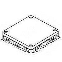
S1V3S344A00A600 Epson, S1V3S344A00A600 Datasheet - Page 40

S1V3S344A00A600
Manufacturer Part Number
S1V3S344A00A600
Description
Telecom Voice Conditioning ICs Voice Guidance IC FLASH
Manufacturer
Epson
Datasheet
1.S1V3S344A00A600.pdf
(44 pages)
Specifications of S1V3S344A00A600
Application
Voice Guidance
Supply Voltage (max)
5 V
Supply Voltage (min)
3.3 V
Maximum Operating Temperature
+ 85 C
Minimum Operating Temperature
- 40 C
Supply Current
0.2 mA
Lead Free Status / RoHS Status
Lead free / RoHS Compliant
9. Reference Material
9.6.2
The power-on reset signal which is input to the NRESET pin changes depending on conditions (power rise time,
component used, board pattern, etc.). Decide the constant of the capacitor and resistor after enough tests have
been completed with the apprication product. With regard to the pull-up resistance of the NRESET pin, if the
impedance is high, noise can generate a malfunction; therefore, the constants must be determined in careful
consideration of resistance value variations.
9.6.3
Sudden power supply variation due to noise may cause malfunction. Consider the following points to prevent
this:
• The power supply should be connected to the HVDD/RVDD and VSS/RVSS pins with patterns as short and
• When connecting between the HVDD/RVDD – VSS/RVSS pins with a bypass capacitor, the HVDD/RVDD
• Connect a 1 µF bypass capacitor between VOUT and RVSS, and connect the VOUT and RVSS pins as short
• Connect a bypass capacitor of at least 4.7 µF between FVOUT and RVSS and ensure that the connection
9.6.4
In order to prevent generation of electromagnetic induction noise caused by mutual inductance, do not arrange a
large current signal line near the circuits that are sensitive to noise such as the oscillation unit.
When a signal line is pallalel with a high-speed line in long distance or intersects a high-speed line, noise may
generated by mutual interference between the signals and it may cause a malfunction. Do not arrange a
high-speed signal line especially near circuits that are sensitive to noise such as the oscillation unit.
36
large as possible.
and VSS/RVSS pins should be connected as short as possible. The bypass capacitor will vary depending on
the system, but should be several μF to several tens of μF.
as possible.
between the FVOUT and RVSS pins is as short as possible.
Reset Circuit
Power Supply Circuit
Arrangement of Signal Lines
4.7μF
4.7μF
1μF
1μF
1μF
Long pattern
Poor example
Figure 9.5 Bypass capacitor connection example
HVDD/RVDD
FVOUT
VSS/RVSS
VOUT
EPSON
Shortest pattern
4.7μF
4.7μF
Good example
S1V3S344 Hardware Specification
1μF
1μF
HVDD/RVDD
FVOUT
VSS/RVSS
VOUT
(Rev. 1.00)


