S1V3S344A00A600 Epson, S1V3S344A00A600 Datasheet
S1V3S344A00A600
Specifications of S1V3S344A00A600


Related parts for S1V3S344A00A600


S1V3S344A00A600 Summary of contents
Page 1
S1V3S344 Hardware Specification Rev. 1.00 ...
Page 2
... Seiko Epson. Seiko Epson reserves the right to make changes to this material without notice. Seiko Epson does not assume any liability of any kind arising out of any inaccuracies contained in this material or due to its application or use in any product or circuit and, further, there is no representation that this material is applicable to products requiring high level reliability, such as, medical products ...
Page 3
... Serial Interface (I2C) ....................................................................................................... 23 7. External Connection Examples................................................................................. 24 7.1 System Clock............................................................................................................................ 24 7.1.1 Direct Input ...................................................................................................................... 24 7.1.2 Oscillator (32.768 kHz) .................................................................................................... 25 7.2 Serial Interface ......................................................................................................................... 26 7.2.1 Clock Synchronous ......................................................................................................... 26 7.2.2 Asynchronous (UART)..................................................................................................... 27 7.2.3 I2C................................................................................................................................... 28 8. Package Dimensions ................................................................................................. 29 8.1 QFP13-52 ................................................................................................................................. 29 S1V3S344 Hardware Specification (Rev. 1.00) Table of Contents EPSON i ...
Page 4
... Clock Direct Input Precautions ................................................................................................. 34 9.6 Precautions on Mounting .......................................................................................................... 35 9.6.1 Oscillation Circuit............................................................................................................. 35 9.6.2 Reset Circuit.................................................................................................................... 36 9.6.3 Power Supply Circuit ....................................................................................................... 36 9.6.4 Arrangement of Signal Lines ........................................................................................... 36 9.6.5 Noise-Induced Erratic Operations ................................................................................... 37 9.6.6 Others.............................................................................................................................. 37 9.7 Product Code Numbering ......................................................................................................... 38 Revision History ............................................................................................................. 39 ii S1V3S344 Hardware Specification EPSON (Rev. 1.00) ...
Page 5
... All the functions are controlled by commands over a serial interface and thus easily added onto any existing systems with a host processor. Using the S1V3S344 allows prompt voice evaluation and reduces the time-to-market for products containing built-in voice guidance functions. S1V3S344 Hardware Specification (Rev. 1.00) *1: The external components differ from those of S1V3034x Series. EPSON 1. Outline 1 ...
Page 6
... Features 2. Features • Audio reproduction − High quality decoding (In EPSON’s original format) − Bit rate: 40 kbps, 32 kbps, 24 kbps, 16 kbps − Sampling rate: 16 kHz • Sequencer Messages − A sequence with phrases can be set (no restriction on phrase combination) − Programmable delay time between phrases 2047 ms (in 1-ms steps) • ...
Page 7
... QFP13-52 VSS 40 STBYEXIT 41 FTVEP0 42 MSGRDY 43 HVDD 44 SOS/TXD 45 SPISWP 46 SIS/RXD/SDA 47 SCKS/SCL 48 NSCSS VSS 52 S1V3S344 Hardware Specification (Rev. 1.00) S1V3S344***** QFP13-52 Figure 3.1 Pinout diagram (QFP13-52) EPSON 3. Pinout Diagram VSS 26 CLKSEL 25 HPOP 24 FTVEP1 23 GPO6 22 GPO5 21 GPO4 20 GPO3 19 GPO2 18 GPO1 17 HPON 16 FSOUT 15 HVDD 14 3 ...
Page 8
... O1 L HVDD IC Z HVDD IC Z HVDD EPSON Function [Clock syncronous] Serial Data Input [Asynchronous] Serial Data Input [I2C] Data input/output [Clock syncronous] Serial Clock Input [Asynchronous] H-level fixed [I2C] Serial Clock Input [Clock syncronous] Serial Data Output [Asynchronous] Serial Data Output ...
Page 9
... IC Z HVDD IC Z HVDD HZTST Z HZTST Z EPSON 4. Pin Description STANDBY mode exit control Input (L: Exit STANDBY mode, H: Continue STANDBY mode) Audio output Audio output (Can be set so that output stops when SNGLEND = H (L level).) Clock input (See section 5.2) Oscillator connector pin (See section 5.2) Oscillator connector pin (See section 5 ...
Page 10
... Internal voltage drop regulator GND General-purpose output pin (Open during normal O operations Unused pins EPSON Test pin (Connected to HVDD during normal operations) Test pin (Connected to HVDD during normal operations) Internal voltage drop regulator output pin (1.8 V) (Connect 1 µF capacitor between VOUT and RVSS ...
Page 11
... DA converter while internally decode-processing the compressed audio data from the internal audio data flash memory or issued from the host. For details of commands, refer to S1V3034x Series Message Protocol Specification and Flash Access Specifications. For more information on voice guidance creation tools, refer to EPSON Speech IC Voice Guidance Creation Tool User Guide. S1V3S344 Hardware Specification (Rev. 1.00) ...
Page 12
... Clock frequency CLKI 32.768 kHz 32.768 kHz input 32.768 kHz L level input 12.288 MHz 12.288 MHz input - EPSON Clock pin settings OSCI OSCO L level input Open Connect 32.768 kHz oscillator L level input Open Must not be selected S1V3S344 Hardware Specification (Rev. 1.00) ...
Page 13
... Table 5.2 Serial interface mode settings Serial interface pin settings SCKS Serial clock input Data input H-level input Data input Serial clock input input/output EPSON 5. Function Description SIS SOS NSCSS Slave Data output selection input Data output L-level input ...
Page 14
... I2C bus rising time exceeds 480 ns due to the load capacity and pull-up resistance. • When using the I2C interface recommended to use the sequence playback. 10 States for NRESET=L (L: L-level output, H: H-level output, Z; High-impedance) SCKS SIS Dependent on NSCSS input level (when NSCSS = L) Z (when NSCSS = EPSON SOS NSCSS S1V3S344 Hardware Specification (Rev. 1.00) ...
Page 15
... HVI VSS HVO VSS -40 write Ta: Read -40 Symbol Min. HVDD 3.0 RVDD 3.0 HVI VSS HVO VSS -40 write Ta: Read -40 EPSON 6. Electrical Characteristics (VSS = 0 V) Rate Value ±10 -65 to +150 (VSS = 0 V) Typ. Max. - 5.5 - 5.5 - HVDD - HVDD - (VSS = 0 V) Typ. Max. ...
Page 16
... Pin names: All input pins Input pin capacitance 12 Condition HVDD=5.5 V RVDD=5.5 V VIN=HVDD or VSS HVDD=5.5 V RVDD=5.5 V HVDD=5.5 V RVDD=5.5 V VIH=HVDD VIL=VSS HVDD=5.5 V HVDD=4.5 V HVDD=5.5 V HVDD=4.5 V HVDD=4.5 V HVDD=4.5 V IOH=-2 mA HVDD=4.5 V IOL=2 mA HVDD=4.5 V IOH=-4 mA HVDD=4.5 V IOL f=1 MHz CI HVDD=RVDD=0 V EPSON Min. Typ. Max 1.0 2 ...
Page 17
... CIO capacitance *1: Approximately current values during decoding under the recommended operating conditions (Ta=25°C) (Audio output has no load.) *2: Static current under the recommended operating conditions (Ta=25°C) S1V3S344 Hardware Specification (Rev. 1.00) f=1 MHz - HVDD=RVDD=0 V f=1 MHz - HVDD=RVDD=0 V EPSON 6. Electrical Characteristics - ...
Page 18
... Pin names: All input pins Input pin capacitance 14 Condition HVDD=3.3V RVDD=3.3V VIN=HVDD or VSS HVDD=3.3V RVDD=3.3V HVDD=3.6 V RVDD=3.6 V VIH=HVDD VIL=VSS HVDD=3.6 V HVDD=3.0 V HVDD=3.6 V HVDD=3.0 V HVDD=3.0 V HVDD=3.0 V IOH=-1.4 mA HVDD=3.0 V IOL=1.4 mA HVDD=3.0 V IOH=-2.8 mA HVDD=3.0 V IOL=2 f=1 MHz CI HVDD=RVDD=0 V EPSON Min. Typ. Max 0.8 1 ...
Page 19
... CIO capacitance *1: Approximately current values during decoding under the recommended operating conditions (Ta=25°C) (Audio output has no load.) *2: Static current under the recommended operating conditions (Ta=25°C) S1V3S344 Hardware Specification (Rev. 1.00) f=1 MHz - HVDD=RVDD=0 V f=1 MHz - HVDD=RVDD=0 V EPSON 6. Electrical Characteristics - ...
Page 20
... Pin names: All input pins Input pin capacitance 16 Condition HVDD=3.0 V RVDD=3.0 V VIN=HVDD or VSS HVDD=3.0 V RVDD=3.0 V HVDD=3.6 V RVDD=3.6 V VIH=HVDD VIL=VSS HVDD=3.6 V HVDD=3.0 V HVDD=3.6 V HVDD=3.0 V HVDD=3.0 V HVDD=3.0 V IOH=-1.4 mA HVDD=3.0 V IOL=1.4 mA HVDD=3.0 V IOH=-2.8 mA HVDD=3.0 V IOL=2 f=1 MHz CI HVDD=RVDD=0 V EPSON Min. Typ. Max 0.8 1 ...
Page 21
... CIO capacitance *1: Approximately current values during decoding under the recommended operating conditions (Ta=25°C) (Audio output has no load.) *2: Static current under the recommended operating conditions (Ta=25°C) S1V3S344 Hardware Specification (Rev. 1.00) f=1 MHz - HVDD=RVDD=0 V f=1 MHz - HVDD=RVDD=0 V EPSON 6. Electrical Characteristics - ...
Page 22
... The jitter characteristics must meet both t Ensure that clock overshoot/undershoot does not exceed absolute maximum ratings in Table 6. PWH PWL OSC t cycle1 Table 6.7 AC characteristics Parameter and t characteristics. Cjper CJcycle EPSON t cycle2 Min. Typ. Max. - 32.768 - - 1/fosc - 0.45*T - 0.55*T osc osc 0.45*T - 0.55*T ...
Page 23
... Ensure that clock overshoot/undershoot does not exceed absolute maximum ratings in Table 6.1. * S1V3S344 Hardware Specification (Rev. 1.00 PWH PWL OSC t cycle1 Table 6.8 System clock timing Parameter and t characteristics. Cjper CJcycle EPSON 6. Electrical Characteristics t cycle2 Min. Typ. Max. - 12.288 - - 1/fosc - 0.45*T - 0.55*T osc osc 0.45*T - ...
Page 24
... HVDD from off to on, due to power supply noise and other factors Figure 6.3 Power on / reset timing Table 6.9 Power on / reset timing Item Input clock source: CLKI Input clock source: OSCI EPSON t 3 Min. Max. Unit μs 100 - ...
Page 25
... There should be no problem about sending padding bytes during the t S1V3S344 Hardware Specification (Rev. 1.00) Hardware Reset ISC_TEST_REQ ISC_TEST_RESP Figure 6.4 Command receipt timing Table 6.10 Command receipt timing Parameter EPSON 6. Electrical Characteristics DEVICE t1 Min. Max. 120 - period. 1 Unit ...
Page 26
... SCKS falling time to SOS going active 7 t NSCSS falling time to SOS going active 8 t NSCSS rising time to SOS going Hi MSB LSB Hi-Z MS LSB Input Data Output Data t8 Active Parameter EPSON t3 Hi-Z t9 Hi-Z Min. Max. 100 - 1.0 - 100 - S1V3S344 Hardware Specification Unit ns μ ...
Page 27
... It should be noted that the numerical values will be greater if the I2C bus rising time exceeds 480 ns *1 due to the load capacity and pull-up resistance. S1V3S344 Hardware Specification (Rev. 1.00 Figure 6.6 I2C timing Table 6.12 Serial interface (I2C) timing Parameter EPSON 6. Electrical Characteristics Min. Max. Unit 12.0 - 6.0 - 6 5.5 2 ...
Page 28
... The OSCEN pin should be set to Low level. The OSCI pin should be set to Low level. The OSCO pin should not be connected. Note that the asynchronous serial interface (UART) is not available if the system clock frequency is set to 12.288 MHz. 24 S1V3S344 S1V3S344 Hardware Specification EPSON (Rev. 1.00) ...
Page 29
... Table 7.1 Typical 32.768 kHz oscillator external circuit constants X’tal Feedback resistance Rd S1V3S344 Hardware Specification (Rev. 1.00) 32.768 kHz oscillator (Epson Toyocom FC-135) Gate capacity Drain capacity Drain resistance EPSON 7. External Connection Examples S1V3S344 Crystal MΩ 200 kΩ ...
Page 30
... MSGRDY output timing, refer to S1V3034x Series Message Protocol Specification. STBYEXIT is an input signal to implement recovery from standby mode to normal operating mode. For more information on STBYEXIT input timing, refer to S1V3034x Series Message Protocol Specification. 26 I/O Port or I/O Port VSS EPSON S1V3S344 SCKS/SCL SOS/TXD SIS/RXD/SDA NSCSS MSGRDY ...
Page 31
... STBYEXIT is an input signal used to implement recovery from standby mode to normal operating mode. For more information on the STBYEXIT input timing, refer to S1V3034x Series Message Protocol Specification. S1V3S344 Hardware Specification (Rev. 1.00) 7. External Connection Examples HVDD SCKS/SCL SOS/TXD SIS/RXD/SDA NSCSS VSS MSGRDY I/O Port STBYEXIT HVDD SHISEL0 SHISEL1 VSS EPSON S1V3S344 27 ...
Page 32
... STBYEXIT is an input signal used to implement recovery from standby mode to normal operating mode. For more information on the STBYEXIT input timing, refer to S1V3034x Series Message Protocol Specification. 28 SCL SCKS/SCL (Open) SOS/TXD SDA SIS/RXD/SDA NSCSS VSS MSGRDY I/O Port STBYEXIT SHISEL0 HVDD SHISEL1 VSS EPSON S1V3S344 S1V3S344 Hardware Specification (Rev. 1.00) ...
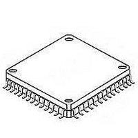
Page 33
... Package Dimensions 8.1 QFP13-52 S1V3S344 Hardware Specification (Rev. 1.00) 8. Package Dimensions EPSON 29 ...
Page 34
... The system clock input unit connection configuration will vary, depending on the clock frequency and clock source used. Refer to section 7.1 for more information. *2: The serial interface connection configuration will vary, depending on the interface type used. Refer to section 7.2 for additional information. 30 S1V3S344 Hardware Specification EPSON (Rev. 1.00) ...
Page 35
... The secondary LPF capacitor (39 nF) GND connection to the VSS should also be as short as possible. The speaker amplifier peripheral circuit and circuit constants shown in Figure 9.2 are provided solely for reference and do not constitute performance guarantees. S1V3S344 Hardware Specification (Rev. 1.00) 9. Reference Material 0.47 μF 1 μF 2.2 μF EPSON 0.1 μF 10 μF 31 ...
Page 36
... STBYEXIT: Low → STANDBY_EXIT_IND received → MUTE released Note: In the above timing chart, the MUTE pin is at the Low level and MUTE is active. * Refer to the Message Protocol Specification for details of standby mode Item Standby mode active period EPSON Min. Max. Unit 150 - ms S1V3S344 Hardware Specification (Rev. 1.00) ...
Page 37
... Never raise the input/output pin voltage level above the supply voltage or above the range specified for electrical characteristics. Avoid lowering below VSS. (2) Make sure the device is not subject to abnormal noise. (3) The potential for unused input pins should be pegged to VDD or VSS. (4) Do not short-circuit the output. S1V3S344 Hardware Specification (Rev. 1.00) 9. Reference Material EPSON 33 ...
Page 38
... The same prevention measures are required for external signals other than the clock external input, but particular caution is necessary for the clock due to the high frequency. Overshoot CLKI waveform Undershoot Figure 9.3 Typical clock input overshoot/undershoot prevention measures 34 Dumping Resistance CLKI Clock Generator EPSON S1V3S344 S1V3S344 Hardware Specification (Rev. 1.00) ...
Page 39
... Do not configure digital signal lines in parallel with components and lines even if such components and lines on other layers. Figure 9.4 Example of oscillation circuit VSS pattern S1V3S344 Hardware Specification (Rev. 1.00) OSCI OSCO VSS EPSON 9. Reference Material 35 ...
Page 40
... Do not arrange a high-speed signal line especially near circuits that are sensitive to noise such as the oscillation unit. 36 Shortest pattern VSS/RVSS HVDD/RVDD VOUT 4.7μF 4.7μF FVOUT EPSON VSS/RVSS HVDD/RVDD 1μF 1μF VOUT FVOUT Good example S1V3S344 Hardware Specification (Rev. 1.00) ...
Page 41
... Electromagnetic induction noise fro the tip of a soldering iron Especially when using a soldering iron, make sure that the IC GND and soldering iron GND are at the same potential before soldering. S1V3S344 Hardware Specification (Rev. 1.00) 9. Reference Material EPSON 37 ...
Page 42
... Reference Material 9.7 Product Code Numbering S1 V 3S34 Package specifications ■ Specifications ■ Built-in voice memory capacity 4: approx. 4 minutes (16 kbps) ■ Product number ■ Product name ■ Product classification S1V3S344 Hardware Specification EPSON (Rev. 1.00) ...
Page 43
... Revision History Date Rev. Page 03/05/2009 1.00 All New S1V3S344 Hardware Specification (Rev. 1.00) Revision details Type First issue EPSON Revision History Details 39 ...
Page 44
... EPSON HONG KONG LTD. 20/F, Harbour Centre, 25 Harbour Road, Wanchai, Hong Kong Phone: +852-2585-4600 FAX: +852-2827-4346 Telex: 65542 EPSCO HX EPSON TAIWAN TECHNOLOGY & TRADING LTD. 14F, No. 7, Song Ren Road, Taipei 110, TAIWAN Phone: +886-2-8786-6688 FAX: +886-2-8786-6660 EPSON SINGAPORE PTE., LTD. ...