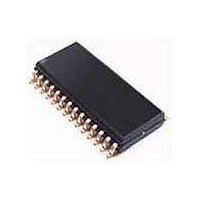
PCK2002MPW NXP Semiconductors, PCK2002MPW Datasheet - Page 8

PCK2002MPW
Manufacturer Part Number
PCK2002MPW
Description
Clock Buffer 14.318-167MHZ I2C 1:10CLK BUFR
Manufacturer
NXP Semiconductors
Datasheet
1.PCK2002MPW-T.pdf
(12 pages)
Specifications of PCK2002MPW
Number Of Outputs
10
Max Input Freq
133 MHz
Propagation Delay (max)
2.7 ns
Supply Voltage (max)
3.465 V
Supply Voltage (min)
3.135 V
Maximum Operating Temperature
+ 70 C
Minimum Operating Temperature
0 C
Mounting Style
SMD/SMT
Package / Case
TSSOP-28
Lead Free Status / RoHS Status
Lead free / RoHS Compliant
Other names
PCK2002MPW,112
1. Inactive means outputs are held LOW and are disabled from switching. These outputs are designed to be configured at power-on and are
1. Inactive means outputs are held LOW and are disabled from switching. These outputs are designed to be configured at power-on and are
1. Inactive means outputs are held LOW and are disabled from switching. These outputs are designed to be configured at power-on and are
Philips Semiconductors
SERIAL CONFIGURATION MAP
The serial bits will be read by the clock buffer in the following order:
All unused register bits (Reserved and N/A) should be designed as “Don’t Care”. It is expected that the controller will force all of these bits to a
“0” level.
All register bits labeled “Initialize to 0” must be written to zero during initialization. Failure to do so may result in a higher than normal operating
current. The controller will read back the last written value.
Byte 0: Output active/inactive register
1 = enable; 0 = disable
NOTE:
Byte 1: Output active/inactive register
1 = enable; 0 = disable
NOTE:
Byte 2: Optional register for possible future requirements
NOTE:
2001 Jul 19
0–300 MHz I
Byte 0 – Bits 7, 6, 5, 4, 3, 2, 1, 0
Byte 1 – Bits 7, 6, 5, 4, 3, 2, 1, 0
Byte 2 – Bits 7, 6, 5, 4, 3, 2, 1, 0
not expected to be configured during the normal modes of operation.
not expected to be configured during the normal modes of operation.
not expected to be configured during the normal modes of operation.
BIT
BIT
BIT
7
6
5
4
3
2
1
0
7
6
5
4
3
2
1
0
7
6
5
4
3
2
1
0
PIN#
PIN#
PIN#
27
26
23
22
18
—
—
—
—
—
—
—
—
11
—
—
—
—
—
—
7
6
3
2
2
C 1:10 clock buffer
BUF_OUT15
BUF_OUT14
BUF_OUT13
BUF_OUT12
BUF_OUT17
BUF_OUT16
BUF_OUT3
BUF_OUT2
BUF_OUT1
BUF_OUT0
(reserved)
(reserved)
(reserved)
(reserved)
(reserved)
(reserved)
NAME
NAME
NAME
—
—
—
—
—
—
—
—
8
DESCRIPTION
DESCRIPTION
DESCRIPTION
Active/Inactive
Active/Inactive
Active/Inactive
Active/Inactive
Active/Inactive
Active/Inactive
Active/Inactive
Active/Inactive
Active/Inactive
Active/Inactive
Initialize to 0
Initialize to 0
Initialize to 0
Initialize to 0
Initialize to 0
Initialize to 0
Initialize to 0
Initialize to 0
(reserved)
(reserved)
(reserved)
(reserved)
(reserved)
(reserved)
PCK2002M
Product data


