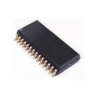
UDA1342TSDB NXP Semiconductors, UDA1342TSDB Datasheet - Page 8

UDA1342TSDB
Manufacturer Part Number
UDA1342TSDB
Description
Audio CODECs AUDIO CODEC MINIDISC
Manufacturer
NXP Semiconductors
Datasheet
1.UDA1342TSN1512.pdf
(45 pages)
Specifications of UDA1342TSDB
Number Of Adc Inputs
4
Number Of Dac Outputs
2
Conversion Rate
110 KSPs
Interface Type
Serial (I2C), L3
Resolution
24 bit
Operating Supply Voltage
2.7 V to 3.6 V
Maximum Operating Temperature
+ 85 C
Mounting Style
SMD/SMT
Package / Case
SSOP-28
Minimum Operating Temperature
- 40 C
Number Of Channels
6
Snr
100 dB
Supply Current
20 mA
Lead Free Status / RoHS Status
Lead free / RoHS Compliant
Other names
UDA1342TS/N1,512
NXP Semiconductors
8
8.1
The UDA1342TS operates in slave mode only, this means
that in all applications the system must provide the system
clock. The system clock frequency is selectable and
depends on the mode of operation:
• L3-bus/I
• Static pin mode: 256f
The system clock must be locked in frequency to the digital
interface signals.
Remarks:
• The bit clock frequency f
• The WS edge MUST fall on the negative edge of the
• The UDA1342TS operates with sample frequencies
2000 Jul 31
handbook, halfpage
other words the bit clock frequency is 128 times the
word select frequency f
BCK signal at all times for proper operation of the digital
interface
from 16 to 110 kHz, however for a system clock of 768f
the sampling frequency must be limited to 55 kHz.
Audio CODEC
FUNCTIONAL DESCRIPTION
System clock
V DDA(ADC)
V SSA(ADC)
2
L3CLOCK
C-bus mode: 256f
L3MODE
SYSCLK
V ADCN
V ADCP
VINR1
VINR2
IPSEL
V DDD
VINL1
VINL2
V SSD
Fig.2 Pin configuration.
10
11
12
13
14
1
2
3
4
5
6
7
8
9
UDA1342TS
s
or 384f
WS
BCK
or less: f
s
, 384f
MGT017
can be up to 128f
s
.
19
18
17
16
15
s
28
27
26
25
24
23
22
21
20
, 512f
BCK
V ref
V SSA(DAC)
VOUTL
V DDA(DAC)
VOUTR
QMUTE
STATUS
STATIC
TEST1
DATAI
DATAO
WS
BCK
L3DATA
≤ 128f
s
or 768f
WS
s
, or in
s
s
8
8.2
The analog front-end of the UDA1342TS consists of two
stereo ADCs with a programmable gain stage (gain from
0 to 24 dB with 3 dB steps) which can be controlled via the
L3-bus/I
8.2.1
In applications in which a 2 V (RMS) input signal is used,
a 15 kΩ resistor must be used in series with the input of the
ADC (see Fig.3). This forms a voltage divider together with
the internal ADC resistor and ensures that only 1 V (RMS)
maximum is input to the IC. Using this application for a
2 V (RMS) input signal, the gain switch must be set to
0 dB. When a 1 V (RMS) input signal is input to the ADC in
the same application, the gain switch must be set to 6 dB.
An overview of the maximum input voltages allowed
against the presence of an external resistor and the setting
of the gain switch is given in Table 1.
Table 1 Application modes using input gain stage
handbook, halfpage
Present
Present
Absent
Absent
RESISTOR
(15 kΩ)
input signal
2 V (RMS)
ADC analog front-end
2
A
C-bus interface.
PPLICATION WITH
Fig.3 Schematic of ADC front-end.
15 kΩ
PGA GAIN
VINL1,
VINR1,
VINL2,
VINR2
0 dB
6 dB
0 dB
6 dB
2 V (RMS)
2,
4,
6,
8
10 kΩ
V ref
UDA1342TS
MAXIMUM INPUT
Product specification
gain = 0 dB
INPUT
UDA1342TS
0.5 V (RMS)
10 kΩ
VOLTAGE
2 V (RMS)
1 V (RMS)
1 V (RMS)
MGT018


