ZXMN6A11ZTA Diodes Zetex, ZXMN6A11ZTA Datasheet
ZXMN6A11ZTA
Specifications of ZXMN6A11ZTA
Available stocks


Related parts for ZXMN6A11ZTA


ZXMN6A11ZTA Summary of contents
Page 1
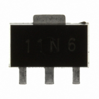
... SOT89 package Applications • DC-DC converters • Power management functions • Disconnect switches • Motor control Ordering information Device Reel size (inches) ZXMN6A11ZTA Device marking 11N6 Issue 2 - September 2006 © Zetex Semiconductors plc 2006 I (A) D 3.6 2.9 Tape width Quantity per (mm) 7 ...
Page 2
Absolute maximum ratings Parameter Drain-source voltage Gate-source voltage Continuous drain current @ (c) Pulsed drain current Continuous source current (body diode) Pulsed source current (body diode) Power dissipation at T =25°C amb Linear derating factor ...
Page 3
Typical characteristics Issue 2 - September 2006 © Zetex Semiconductors plc 2006 ZXMN6A11Z 3 www.zetex.com ...
Page 4
Electrical characteristics (@ T Parameter Static Drain-source breakdown voltage V Zero gate voltage drain current Gate-body leakage Gate-source threshold voltage Static drain-source on-state (*) resistance (*)(‡) Forward transconductance (‡) Dynamic Input capacitance Output capacitance Reverse transfer capacitance (†) (‡) Switching ...
Page 5
Typical characteristics Issue 2 - September 2006 © Zetex Semiconductors plc 2006 ZXMN6A11Z 5 www.zetex.com ...
Page 6
Typical characteristics Charge Basic gate charge waveform V DS 90% 10 d(on (on) Switching time waveforms Issue 2 - September 2006 © Zetex Semiconductors plc 2006 ...
Page 7
Issue 2 - September 2006 © Zetex Semiconductors plc 2006 Intentionally left blank 7 ZXMN6A11Z www.zetex.com ...
Page 8
Package outline - SOT89 DIM Millimeters Min Max A 1.40 1.60 B 0.44 0.56 B1 0.36 0.48 C 0.35 0.44 D 4.40 4.60 D1 1.52 1.83 Note: Controlling dimensions are in millimeters. Approximate dimensions ...