AO7600 Alpha & Omega Semiconductor Inc, AO7600 Datasheet
AO7600
Specifications of AO7600
Available stocks


Related parts for AO7600


AO7600 Summary of contents
Page 1
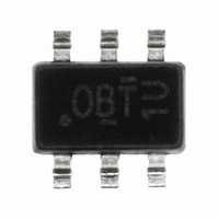
... The DS(ON) complementary MOSFETs may be used to form a level shifted high side switch, an inverter, and for a host of other applications. Both devices are ESD protected. AO7600 and AO7600L are electrically identical. -RoHS Compliant -AO7600L is Halogen Free SC-70-6 (SOT-323) Top View ...
Page 2
... AO7600 N-Channel: Electrical Characteristics (T Symbol Parameter STATIC PARAMETERS BV Drain-Source Breakdown Voltage DSS I Zero Gate Voltage Drain Current DSS I Gate-Body leakage current GSS V Gate Threshold Voltage GS(th state drain current D(ON) R Static Drain-Source On-Resistance DS(ON) g Forward Transconductance FS V Diode Forward Voltage SD Maximum Body-Diode Continuous Current ...
Page 3
... AO7600 N-Channel: TYPICAL ELECTRICAL AND THERMAL CHARACTERISTICS 10 10V (Volts) DS Fig 1: On-Region Characteristics 480 440 V =1.8V GS 400 360 320 V =2.5V GS 280 240 200 160 (A) D Figure 3: On-Resistance vs. Drain Current and Gate Voltage 500 460 420 380 340 300 260 220 180 140 ...
Page 4
... AO7600 N-Channel: TYPICAL ELECTRICAL AND THERMAL CHARACTERISTICS 5 V =10V =0. 0.0 0.2 0.4 0.6 0.8 1.0 1.2 1.4 1.6 1.8 2.0 Q (nC) g Figure 7: Gate-Charge Characteristics 10.0 T =150°C, T =25°C J(Max DS(ON) 10ms limited 1.0 0.1s 1s 0.1 10s DC 0.0 0 (Volts) DS Figure 9: Maximum Forward Biased Safe ...
Page 5
... AO7600 P-Channel Electrical Characteristics (T Symbol Parameter STATIC PARAMETERS BV Drain-Source Breakdown Voltage DSS I Zero Gate Voltage Drain Current DSS I Gate-Body leakage current GSS V Gate Threshold Voltage GS(th state drain current D(ON) R Static Drain-Source On-Resistance DS(ON) g Forward Transconductance FS V Diode Forward Voltage SD I Maximum Body-Diode Continuous Current ...
Page 6
... AO7600 P-Channel: TYPICAL ELECTRICAL AND THERMAL CHARACTERISTICS 6 -10V (Volts) DS Fig 1: On-Region Characteristics 900 V =-1.8V GS 800 700 V GS 600 500 400 300 (A) D Figure 3: On-Resistance vs. Drain Current and Gate Voltage 900 800 700 125°C 600 500 25°C 400 300 (Volts) GS Figure 5: On-Resistance vs. Gate-Source Voltage Alpha & ...
Page 7
... AO7600 P-Channel: TYPICAL ELECTRICAL AND THERMAL CHARACTERISTICS 5 V =-10V DS I =-0. 0.0 0.5 1.0 -Q (nC) g Figure 7: Gate-Charge Characteristics 10.00 T =150°C, T =25°C J(Max DS(ON) 1.00 limited 0.10 1s 10s 0.01 0.00 0 (Volts) DS Figure 9: Maximum Forward Biased Safe Operating Area (Note E) 10 D=T ...