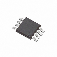
ZXMD63P02XTC Diodes Zetex, ZXMD63P02XTC Datasheet

ZXMD63P02XTC
Specifications of ZXMD63P02XTC
Related parts for ZXMD63P02XTC
ZXMD63P02XTC Summary of contents
Page 1
... Low gate drive Low profile SOIC package APPLICATIONS Converters Power Management Functions Disconnect switches Motor control ORDERING INFORMATION DEVICE REEL SIZE (inches) ZXMD63P02XTA 7 ZXMD63P02XTC 13 DEVICE MARKING ZXM63P02 ISSUE 1 - JUNE 2004 =-1.7A D TAPE WIDTH (mm) QUANTITY PER REEL 12mm embossed 1000 units 12mm embossed ...
Page 2
ZXMD63P02X ABSOLUTE MAXIMUM RATINGS. PARAMETER Drain-Source Voltage Gate- Source Voltage Continuous Drain Current (V =4.5V =4.5V Pulsed Drain Current (c)(d) Continuous Source Current (Body Diode)(b)(d) Pulsed Source Current (Body Diode)(c)(d) Power Dissipation at T =25°C ...
Page 3
Refer Note ( 100ms 10ms 1ms 100µs 0.1 0 Drain-Source Voltage (V) DS Safe Operating Area 120 Refer Note (b) 100 80 60 D=0.5 40 D=0.2 20 D=0.1 D=0.05 Single Pulse 0 ...
Page 4
ZXMD63P02X ELECTRICAL CHARACTERISTICS (at T PARAMETER STATIC Drain-Source Breakdown Voltage Zero Gate Voltage Drain Current Gate-Body Leakage Gate-Source Threshold Voltage Static Drain-Source On-State Resistance (1) Forward Transconductance (3) DYNAMIC (3) Input Capacitance Output Capacitance Reverse Transfer Capacitance SWITCHING(2) (3) Turn-On ...
Page 5
C 4. 0.1 0 Drain-Source Voltage (V) DS Output Characteristics 10 VDS=-10V T=150 C T= 0.1 1 1 Gate-Source Voltage (V) GS Typical Transfer Characteristics 10 ...
Page 6
ZXMD63P02X 700 600 500 400 300 200 100 0 0 Drain Source Voltage (V) DS Capacitance v Drain-Source Voltage Basic Gate Charge Waveform Switching Time Waveforms ISSUE 1 - JUNE 2004 TYPICAL CHARACTERISTICS 5 Vgs=0V f=1Mhz 4.5 ...
Page 7
ZXMD63P02X PACKAGE DIMENSIONS Conforms to JEDEC MO-187 Iss A PAD LAYOUT DETAILS Zetex plc. Fields New Road, Chadderton, Oldham, OL9-8NP, United Kingdom. Telephone: (44)161 622 4422 ...


