SI8901EDB-T2-E1 Vishay, SI8901EDB-T2-E1 Datasheet

MOSFET BIDIR P-CH 20V 2X3 6-MFP

SI8901EDB-T2-E1

Manufacturer Part Number
SI8901EDB-T2-E1
Description
MOSFET BIDIR P-CH 20V 2X3 6-MFP
Manufacturer
Vishay
Series
TrenchFET®r
Datasheet

Specifications of SI8901EDB-T2-E1

Fet Type
2 P-Channel (Dual)
Fet Feature
Logic Level Gate
Rds On (max) @ Id, Vgs
60 mOhm @ 1A, 4.5V
Drain To Source Voltage (vdss)
20V
Current - Continuous Drain (id) @ 25° C
3.5A
Vgs(th) (max) @ Id
1V @ 350µA
Power - Max
1W
Mounting Type
Surface Mount
Package / Case
6-MICRO FOOT®CSP
Transistor Polarity
P Channel
Continuous Drain Current Id
-4.4A
Drain Source Voltage Vds
-20V
On Resistance Rds(on)
105mohm
Rds(on) Test Voltage Vgs
12V
Threshold Voltage Vgs Typ
-1V
Lead Free Status / RoHS Status
Lead free / RoHS Compliant
Gate Charge (qg) @ Vgs
-
Lead Free Status / RoHS Status
Lead free / RoHS Compliant, Lead free / RoHS Compliant
Other names
SI8901EDB-T2-E1TR

Available stocks

Company
Part Number
Manufacturer
Quantity
Price
Part Number:
SI8901EDB-T2-E1
Manufacturer:
VISHAY/威世
Quantity:
20 000
Company:
Part Number:
SI8901EDB-T2-E1
Quantity:
3 000
Notes:
a. Surface Mounted on 1" x 1" FR4 board.
b. The foot is defined as the top surface of the package.
c. Refer to IPC/JEDEC (J-STD-020C), no manual or hand soldering.
Document Number: 72941
S-82119-Rev. C, 08-Sep-08
ABSOLUTE MAXIMUM RATINGS T
Parameter
Source1- Source2 Voltage
Gate-Source Voltage
Continuous Source1- Source2 Current (T
Pulsed Source1- Source2 Current
Maximum Power Dissipation
Operating Junction and Storage Temperature Range
Package Reflow Conditions
THERMAL RESISTANCE RATINGS
Parameter
Maximum Junction-to-Ambient
Maximum Junction-to-Foot
PRODUCT SUMMARY
V
S1S2
G
- 20
Bump Side View
S
S
2
1
2
(V)
1
5
6
4
3
2
G
S
S
2
1
1
0.060 at V
0.080 at V
0.105 at V
Bi-Directional P-Channel 20-V (D-S) MOSFET
MICRO FOOT
R
b
S1S2(on)
c
a
a
GS
GS
GS
= - 4.5 V
= - 2.5 V
= - 1.8 V
(Ω)
J
Backside View
= 150 °C)
A
a
I
S1S2
= 25 °C, unless otherwise noted
- 4.4
- 3.9
- 3.4
IR/Convection
Steady State
Steady State
T
T
T
T
A
A
A
A
(A)
t ≤ 5 s
= 25 °C
= 85 °C
= 25 °C
= 85 °C
Device Marking:
8901E = P/N Code
xxx = Date/Lot Traceability Code
Ordering Information:
Si8901EDB-T2-E1 (Lead (Pb)-free)
Pin 1 Identifier
FEATURES
APPLICATIONS
• TrenchFET
• Ultra-Low R
• ESD Protected: 6000 V
• MICRO FOOT
• Smart Batteries for Portable Devices
Symbol
Symbol
T
V
I
R
R
J
Reduces Footprint Area, Profile (0.65 mm)
and On-Resistance Per Footprint Area
V
S1S2
I
S1S2
P
, T
SM
thJA
thJF
GS
D
stg
®
SS(on)
Power MOSFET
Typical
®
- 4.4
- 3.2
5 s
1.7
0.8
60
95
18
Chipscale Packaging
- 55 to 150
G
G
1
2
± 12
- 20
- 10
260
Steady State
Maximum
- 3.5
- 2.5
120
0.5
75
22
5.4 kΩ
5.4 kΩ
Vishay Siliconix
1
Si8901EDB
P-Channel
www.vishay.com
°C/W
Unit
Unit
°C
W
V
A
S
S
RoHS
COMPLIANT
1
2
1

Related parts for SI8901EDB-T2-E1

SI8901EDB-T2-E1 Summary of contents

Page 1

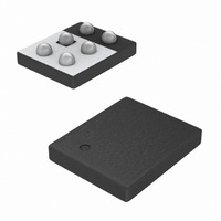
... Reduces Footprint Area, Profile (0.65 mm) - 3.4 and On-Resistance Per Footprint Area APPLICATIONS • Smart Batteries for Portable Devices Backside View Pin 1 Identifier Device Marking: 8901E = P/N Code xxx = Date/Lot Traceability Code Ordering Information: Si8901EDB-T2-E1 (Lead (Pb)-free °C, unless otherwise noted A Symbol V S1S2 °C A ...

Page 2

... Si8901EDB Vishay Siliconix SPECIFICATIONS °C, unless otherwise noted J Parameter Static Gate Threshold Voltage Gate-Body Leakage Zero Gate Voltage Source Current a On-State Source Current a Source1- Source2 On-State Resistance a Forward Transconductance b Dynamic Turn-On Delay Time Rise Time Turn-Off Delay Time Fall Time Notes: a. Pulse test ...

Page 3

... A S1S2 0.12 0.08 0.04 0. Gate-to-Source Voltage (V) GS On-Resistance vs. Gate-to-Source Voltage Document Number: 72941 S-82119-Rev. C, 08-Sep-08 1.5 V 2.0 2 Si8901EDB Vishay Siliconix 125 ° ° °C 0 0.0 0.4 0.8 1 Gate-to-Source Voltage (V) GS Transfer Characteristics 1 4 S1S2 1.4 1.2 1.0 0.8 ...

Page 4

... Si8901EDB Vishay Siliconix TYPICAL CHARACTERISTICS 25 °C, unless otherwise noted 0.01 0.1 1 Time (s) Single Pulse Power, Junction-to-Ambient 2 1 Duty Cycle = 0.5 0.2 0.1 0.1 0.05 0.02 Single Pulse 0. Duty Cycle = 0.5 0.2 0.1 0.1 0.05 0.02 Single Pulse 0. www.vishay.com 4 10 100 1000 ...

Page 5

... Technology and Package Reliability represent a composite of all qualified locations. For related documents such as package/tape drawings, part marking, and reliability data, see http://www.vishay.com/ppg?72941. Document Number: 72941 S-82119-Rev. C, 08-Sep-08 ∼ 0.30 0. Millimeters Max. 0.650 0.290 0.360 0.410 1.6 2.4 0.850 0.400 Si8901EDB Vishay Siliconix Note Diameter Bump Note Inches Min. ...

Page 6

... Vishay product could result in personal injury or death. Customers using or selling Vishay products not expressly indicated for use in such applications their own risk and agree to fully indemnify and hold Vishay and its distributors harmless from and against any and all claims, liabilities, expenses and damages arising or resulting in connection with such use or sale, including attorneys fees, even if such claim alleges that Vishay or its distributor was negligent regarding the design or manufacture of the part ...

Related keywords