IRF7342TRPBF International Rectifier, IRF7342TRPBF Datasheet
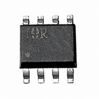
MOSFET 2P-CH 55V 3.4A 8-SOIC

IRF7342TRPBF

Manufacturer Part Number
IRF7342TRPBF
Description
MOSFET 2P-CH 55V 3.4A 8-SOIC
Manufacturer
International Rectifier
Series
HEXFET®r
Type
Power MOSFETr

Specifications of IRF7342TRPBF

Fet Type
2 P-Channel (Dual)
Fet Feature
Logic Level Gate
Rds On (max) @ Id, Vgs
105 mOhm @ 3.4A, 10V
Drain To Source Voltage (vdss)
55V
Current - Continuous Drain (id) @ 25° C
3.4A
Vgs(th) (max) @ Id
1V @ 250µA
Gate Charge (qg) @ Vgs
38nC @ 10V
Input Capacitance (ciss) @ Vds
690pF @ 25V
Power - Max
2W
Mounting Type
Surface Mount
Package / Case
8-SOIC (3.9mm Width)
Channel Type
P
Current, Drain
-3.4 A
Gate Charge, Total
26 nC
Package Type
SO-8
Polarization
Dual P-Channel
Power Dissipation
2 W
Resistance, Drain To Source On
0.170 Ohm
Temperature, Operating, Maximum
+150 °C
Temperature, Operating, Minimum
-55 °C
Time, Turn-off Delay
43 ns
Time, Turn-on Delay
14 ns
Transconductance, Forward
3.3 S
Voltage, Breakdown, Drain To Source
-55 V
Voltage, Drain To Source
–55 V
Voltage, Forward, Diode
-1.2 V
Voltage, Gate To Source
±20 V
Number Of Elements
2
Polarity
P
Channel Mode
Enhancement
Drain-source On-res
0.105Ohm
Drain-source On-volt
55V
Gate-source Voltage (max)
±20V
Continuous Drain Current
3.4A
Operating Temp Range
-55C to 150C
Operating Temperature Classification
Military
Mounting
Surface Mount
Pin Count
8
Configuration
Dual
Transistor Polarity
Dual P-Channel
Drain-source Breakdown Voltage
- 55 V
Gate-source Breakdown Voltage
20 V
Mounting Style
SMD/SMT
Gate Charge Qg
26 nC
Lead Free Status / RoHS Status
Lead free / RoHS Compliant
Other names
IRF7342PBFTR

Available stocks

Company
Part Number
Manufacturer
Quantity
Price
Part Number:
IRF7342TRPBF
Manufacturer:
IR
Quantity:
20 000
Part Number:
IRF7342TRPBF
0
Company:
Part Number:
IRF7342TRPBF
Quantity:
651
Company:
Part Number:
IRF7342TRPBF
Quantity:
4 000
Company:
Part Number:
IRF7342TRPBF
Quantity:
5 000
Company:
Part Number:
IRF7342TRPBF
Quantity:
24 000
Description
Fifth Generation HEXFETs from International Rectifier
utilize advanced processing techniques to achieve
extremely low on-resistance per silicon area. This
benefit, combined with the fast switching speed and
ruggedized device design that HEXFET Power
MOSFETs are well known for, provides the designer
with an extremely efficient and reliable device for use
in a wide variety of applications.
The SO-8 has been modified through a customized
leadframe for enhanced thermal characteristics and
multiple-die capability making it ideal in a variety of
power applications. With these improvements, multiple
devices can be used in an application with dramatically
reduced board space. The package is designed for
vapor phase, infra red, or wave soldering techniques.
Power dissipation of greater than 0.8W is possible in
a typical PCB mount application.
Absolute Maximum Ratings
Thermal Resistance
www.irf.com
R
V
I
I
I
P
P
V
V
E
dv/dt
T
D
D
DM
J,
DS
D
D
GS
GSM
AS
@ T
@ T
JA
@T
@T
T
Generation V Technology
Ultra Low On-Resistance
Dual P-Channel Mosfet
Surface Mount
Available in Tape & Reel
Dynamic dv/dt Rating
Fast Switching
STG
C
C
C
C
= 25°C
= 70°C
= 25°C
= 70°C
Maximum Junction-to-Ambient
Drain- Source Voltage
Continuous Drain Current, V
Pulsed Drain Current
Power Dissipation
Power Dissipation
Linear Derating Factor
Gate-to-Source Voltage
Gate-to-Source Voltage Single Pulse tp<10µs
Single Pulse Avalanche Energy
Peak Diode Recovery dv/dt
Junction and Storage Temperature Range
Parameter
Parameter
GS
GS
@ 10V
@ 10V
G 2
G 1
S2
S 1
1
2
3
4
T op V iew
Typ.
–––
HEXFET
8
7
6
5
-55 to + 150
Max.
0.016
D 1
D 1
D 2
-3.4
-2.7
± 20
114
D 2
-55
-27
2.0
1.3
5.0
30
S O -8
®
R
IRF7342
DS(on)
Power MOSFET
V
Max.
62.5
DSS
= 0.105
= -55V
PD -91859
Units
Units
W/°C
°C/W
V/ns
W
°C
V
A
V
V
1
2/24/99

Related parts for IRF7342TRPBF

IRF7342TRPBF Summary of contents

Page 1

... Available in Tape & Reel Dynamic dv/dt Rating Fast Switching Description Fifth Generation HEXFETs from International Rectifier utilize advanced processing techniques to achieve extremely low on-resistance per silicon area. This benefit, combined with the fast switching speed and ruggedized device design that HEXFET Power ...

Page 2

IRF7342 Electrical Characteristics @ T Parameter V Drain-to-Source Breakdown Voltage (BR)DSS Breakdown Voltage Temp. Coefficient (BR)DSS J R Static Drain-to-Source On-Resistance DS(on) V Gate Threshold Voltage GS(th) g Forward Transconductance fs I Drain-to-Source Leakage Current DSS Gate-to-Source ...

Page 3

VGS TOP -15V -12V -10V -8.0V -6.0V -4.5V -4.0V -3.5V BOTTOM -3.0V 10 -3.0V 1 20µs PULSE WIDTH 0.1 0 Drain-to-Source Voltage (V) DS Fig 1. Typical Output Characteristics 100 ...

Page 4

IRF7342 2.0 -3 1.5 1.0 0.5 0.0 -60 -40 - Junction Temperature ( C) J Fig 5. Normalized On-Resistance Vs. Temperature ...

Page 5

1MHz iss rss 960 oss iss 720 480 C oss 240 C rss ...

Page 6

IRF7342 SO-8 Package Details 0 ...

Page 7

Tape and Reel . . ...

Related keywords