SP8M4TB Rohm Semiconductor, SP8M4TB Datasheet
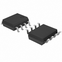
MOSFET N+P 30V 9A/7A 8-SOIC

SP8M4TB

Manufacturer Part Number
SP8M4TB
Description
MOSFET N+P 30V 9A/7A 8-SOIC
Manufacturer
Rohm Semiconductor
Datasheet

Specifications of SP8M4TB

Fet Type
N and P-Channel
Fet Feature
Logic Level Gate
Rds On (max) @ Id, Vgs
18 mOhm @ 9A, 10V
Drain To Source Voltage (vdss)
30V
Current - Continuous Drain (id) @ 25° C
9A, 7A
Vgs(th) (max) @ Id
2.5V @ 1mA
Gate Charge (qg) @ Vgs
15nC @ 5V
Input Capacitance (ciss) @ Vds
1190pF @ 10V
Power - Max
2W
Mounting Type
Surface Mount
Package / Case
8-SOIC (3.9mm Width)
Configuration
Dual Dual Drain
Transistor Polarity
N and P-Channel
Resistance Drain-source Rds (on)
0.018 Ohms
Drain-source Breakdown Voltage
30 V
Gate-source Breakdown Voltage
+/- 20 V
Continuous Drain Current
9 A, - 7 A
Power Dissipation
2 W
Mounting Style
SMD/SMT
Fall Time
22 ns, 70 ns
Rise Time
15 ns, 50 ns
Lead Free Status / RoHS Status
Lead free / RoHS Compliant
Other names
SP8M4TBTR
Transistors
Switching
SP8M4
1) Low on-resistance.
2) Built-in G-S Protection Diode.
3) Small and Surface Mount Package (SOP8).
Power switching, DC / DC converter.
∗1 Pw≤10µs, Duty cycle≤1%
∗2 MOUNTED ON A CERAMIC BOARD.
Channel to ambient
∗MOUNTED ON A CERAMIC BOARD.
Drain-source voltage
Gate-source voltage
Drain current
Source current
(Body diode)
Total power dissipation
Channel temperature
Storage temperature
Features
Application
Absolute maximum ratings (Ta=25°C)
Thermal resistance (Ta=25°C)
Parameter
Parameter
Continuous
Pulsed
Continuous
Pulsed
Symbol
V
V
Tstg
Tch
I
I
P
DSS
GSS
I
DP
I
SP
Rth (ch-a)
D
S
D
Symbol
Nchannel
±9.0
±36
1.6
30
20
36
−55 to +150
Limits
Limits
150
62.5
2
Pchannel
±7.0
−1.6
−30
−20
±28
−28
External dimensions (Unit : mm)
SOP8
°C / W
Unit
Unit
°C
°C
W
V
V
A
A
A
A
∗1
∗1
∗2
∗A protection diode is included between the gate and
∗2
the source terminals to protect the diode against static
electricity when the product is in use. Use the protection
circuit when the fixed voltages are exceeded.
∗1 ESD PROTECTION DIODE
∗2 BODY DIODE
Equivalent circuit
(8)
(1)
1.27
5.0±0.2
∗1
(7)
(2)
0.1
Each lead has same dimensions
0.4±0.1
∗2
(6)
(3)
∗1
Rev.A
0.2±0.1
(5)
(4)
(1) Tr1 (Nch) Source
(2) Tr1 (Nch) Gate
(3) Tr2 (Pch) Source
(4) Tr2 (Pch) Gate
(5) Tr2 (Pch) Drain
(6) Tr2 (Pch) Drain
(7) Tr1 (Nch) Drain
(8) Tr1 (Nch) Drain
(1) (2) (3) (4)
(8) (7) (6) (5)
SP8M4
1/5

Related parts for SP8M4TB

SP8M4TB Summary of contents

Page 1

Transistors Switching SP8M4 Features 1) Low on-resistance. 2) Built-in G-S Protection Diode. 3) Small and Surface Mount Package (SOP8). Application Power switching converter. Absolute maximum ratings (Ta=25°C) Parameter Symbol Drain-source voltage V DSS Gate-source voltage V GSS ...

Page 2

Transistors N-ch Electrical characteristics (Ta=25°C) Parameter Symbol Gate-source leakage I GSS Drain-source breakdown voltage V (BR) DSS Zero gate voltage drain current I DSS Gate threshold voltage V GS (th) Static drain-source on-state R DS (on) resistance Forward transfer admittance ...

Page 3

Transistors P-ch Electrical characteristics (Ta=25°C) Parameter Symbol Gate-source leakage I GSS Drain-source breakdown voltage V (BR) DSS Zero gate voltage drain current I DSS Gate threshold voltage V GS (th) Static drain-source on-state R DS (on) resistance Forward transfer admittance ...

Page 4

Transistors N-ch Electrical characteristic curves 10000 Ta=25°C f=1MHz = 1000 C iss C oss C rss 100 10 0.01 0 100 DRAIN-SOURCE VOLTAGE : V (V) DS Fig.1 Typical Capacitance vs. Drain-Source Voltage 10 =10V V ...

Page 5

Transistors P-ch Electrical characteristic curves 10000 Ta=25°C f=1MHz = iss 1000 C oss C rss 100 0.01 0 100 DRAIN-SOURCE VOLTAGE : −V (V) DS Fig.1 Typical Capacitance vs. Drain-Source Voltage 10 = −10V V ...

Page 6

Appendix No technical content pages of this document may be reproduced in any form or transmitted by any means without prior permission of ROHM CO.,LTD. The contents described herein are subject to change without notice. The specifications for the product ...

Related keywords