SI5515DC-T1-E3 Vishay, SI5515DC-T1-E3 Datasheet - Page 11
SI5515DC-T1-E3
Manufacturer Part Number
SI5515DC-T1-E3
Description
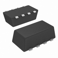
MOSFET N/P-CH 20V CHIPFET 1206-8
Manufacturer
Vishay
Series
TrenchFET®r
Specifications of SI5515DC-T1-E3
Fet Type
N and P-Channel
Fet Feature
Logic Level Gate
Rds On (max) @ Id, Vgs
40 mOhm @ 4.4A, 4.5V
Drain To Source Voltage (vdss)
20V
Current - Continuous Drain (id) @ 25° C
4.4A, 3A
Vgs(th) (max) @ Id
1V @ 250µA
Gate Charge (qg) @ Vgs
7.5nC @ 4.5V
Power - Max
1.1W
Mounting Type
Surface Mount
Package / Case
1206-8 ChipFET™
Transistor Polarity
N And P Channel
Continuous Drain Current Id
4.4A
Drain Source Voltage Vds
20V
On Resistance Rds(on)
32mohm
Rds(on) Test Voltage Vgs
4.5V
Threshold Voltage Vgs Typ
400mV
Lead Free Status / RoHS Status
Lead free / RoHS Compliant
Other names
SI5515DC-T1-E3TR
Available stocks
Company
Part Number
Manufacturer
Quantity
Price
Company:

Part Number:
SI5515DC-T1-E3
Manufacturer:
Vishay/Siliconix
Quantity:
32 095
Part Number:
SI5515DC-T1-E3
Manufacturer:
VISHY
Quantity:
20 000


AN812
Vishay Siliconix
THERMAL PERFORMANCE
Junction-to-Foot Thermal Resistance (the Package
Performance)
Thermal performance for the 1206-8 ChipFET measured as
junction-to-foot thermal resistance is 30_C/W typical, 40_C/W
maximum for the dual device. The “foot” is the drain lead of the
device as it connects with the body. This is identical to the dual
SO-8 package R
shortening the leads to the point where they become only a
small part of the total footprint area.
Junction-to-Ambient Thermal Resistance
(dependent on pcb size)
The typical R
90_C/W steady state, identical to the SO-8. Maximum ratings
are 110_C/W for both the 1206-8 and the SO-8. Both packages
have comparable thermal performance on the 1” square pcb
footprint with the 1206-8 dual package having a quarter of the
body area, a significant factor when considering board area.
Testing
To aid comparison further, Figure 4 illustrates ChipFET 1206-8
dual thermal performance on two different board sizes and
three different pad patterns.The results display the thermal
performance out to steady state and produce a graphic
account on how an increased copper pad area for the drain
connections can enhance thermal performance. The
measured steady state values of R
ChipFET are :
www.vishay.com
2
1) Minimum recommended pad pattern (see
Figure 2) on the evaluation board size of
0.5 in x 0.6 in.
2) The evaluation board with the pad pattern
described on Figure 3.
3) Industry standard 1” square pcb with
maximum copper both sides.
Front of Board
Qja
ChipFETr
Qjf
for the dual-channel 1206-8 ChipFET is
performance, a feat made possible by
Qja
for the Dual 1206-8
185_C/W
128_C/W
90_C/W
FIGURE 3.
The results show that a major reduction can be made in the
thermal resistance by increasing the copper drain area. In this
example, a 57_C/W reduction was achieved without having to
increase the size of the board. If increasing board size is an
option, a further 38_C/W reduction was obtained by
maximizing the copper from the drain on the larger 1” square
PCB.
SUMMARY
The thermal results for the dual-channel 1206-8 ChipFET
package display identical power dissipation performance to
the SO-8 with a footprint reduction of 80%. Careful design of
the package has allowed for this performance to be achieved.
The short leads allow the die size to be maximized and thermal
resistance to be reduced within the confines of the TSOP-6
body size.
ASSOCIATED DOCUMENT
1206-8 ChipFET Single Thermal performance, AN811,
(http://www.vishay.com/doc?71126).
Back of Board
200
160
120
80
40
0
10
-5
10
FIGURE 4.
-4
10
vishay.com
-3
10
-2
Time (Secs)
Dual 1206-8 ChipFET
10
-1
Min. Footprint
1
1” Square PCB
Document Number: 71127
10
100
Dual EVB
12-Dec-03
1000
Related parts for SI5515DC-T1-E3
Image
Part Number
Description
Manufacturer
Datasheet
Request
R

Part Number:
Description:
N/P-Ch 1206-8 ChipFET 20V 40/86mohm @ 4.5V
Manufacturer:
Vishay
Part Number:
Description:
Complementary 20-v D-s Mosfet
Manufacturer:
Vishay
Datasheet:
Part Number:
Description:
357-036-542-201 CARDEDGE 36POS DL .156 BLK LOPRO
Manufacturer:
Vishay
Datasheet:
Part Number:
Description:
357-036-542-201 CARDEDGE 36POS DL .156 BLK LOPRO
Manufacturer:
Vishay
Datasheet:
Part Number:
Description:
357-036-542-201 CARDEDGE 36POS DL .156 BLK LOPRO
Manufacturer:
Vishay
Datasheet:
Part Number:
Description:
357-036-542-201 CARDEDGE 36POS DL .156 BLK LOPRO
Manufacturer:
Vishay
Datasheet:
Part Number:
Description:
357-036-542-201 CARDEDGE 36POS DL .156 BLK LOPRO
Manufacturer:
Vishay
Datasheet:
Part Number:
Description:
357-036-542-201 CARDEDGE 36POS DL .156 BLK LOPRO
Manufacturer:
Vishay
Datasheet:
Part Number:
Description:
357-036-542-201 CARDEDGE 36POS DL .156 BLK LOPRO
Manufacturer:
Vishay
Datasheet:
Part Number:
Description:
357-036-542-201 CARDEDGE 36POS DL .156 BLK LOPRO
Manufacturer:
Vishay
Datasheet:
Part Number:
Description:
357-036-542-201 CARDEDGE 36POS DL .156 BLK LOPRO
Manufacturer:
Vishay
Datasheet:
Part Number:
Description:
357-036-542-201 CARDEDGE 36POS DL .156 BLK LOPRO
Manufacturer:
Vishay
Datasheet:
Part Number:
Description:
357-036-542-201 CARDEDGE 36POS DL .156 BLK LOPRO
Manufacturer:
Vishay
Datasheet:
Part Number:
Description:
357-036-542-201 CARDEDGE 36POS DL .156 BLK LOPRO
Manufacturer:
Vishay
Datasheet:
Part Number:
Description:
357-036-542-201 CARDEDGE 36POS DL .156 BLK LOPRO
Manufacturer:
Vishay
Datasheet: