PMBFJ176,215 NXP Semiconductors, PMBFJ176,215 Datasheet
PMBFJ176,215
Specifications of PMBFJ176,215
933908920215
PMBFJ176 T/R


Related parts for PMBFJ176,215


PMBFJ176,215 Summary of contents
Page 1
DATA SHEET PMBFJ174 to 177 P-channel silicon field-effect transistors Product specification DISCRETE SEMICONDUCTORS April 1995 ...
Page 2
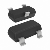
... NXP Semiconductors P-channel silicon field-effect transistors DESCRIPTION Silicon symmetrical p-channel junction FETs in plastic microminiature SOT23 envelopes.They are intended for application with analogue switches, choppers, commutators etc. using SMD technology. A special feature is the interchangeability of the drain and source connections. PINNING 1 = drain 2 = source ...
Page 3
... NXP Semiconductors P-channel silicon field-effect transistors RATINGS Limiting values in accordance with the Absolute Maximum System (IEC 134) Drain-source voltage Gate-source voltage Gate-drain voltage Gate current (d.c.) Total power dissipation = 25 C ( amb Storage temperature range Junction temperature THERMAL RESISTANCE From junction to ambient in free air STATIC CHARACTERISTICS = 25 ...
Page 4
... NXP Semiconductors P-channel silicon field-effect transistors DYNAMIC CHARACTERISTICS = 25 C unless otherwise specified T j Input capacitance MHz Feedback capacitance MHz Switching times (see Fig.2 3) Delay time Rise time Turn-on time Storage temperature Fall time Turn-off time Test conditions: −V DD handbook, halfpage 50 Ω ...
Page 5
... NXP Semiconductors P-channel silicon field-effect transistors PACKAGE OUTLINE Plastic surface-mounted package; 3 leads DIMENSIONS (mm are the original dimensions UNIT max. 1.1 0.48 0.15 mm 0.1 0.9 0.38 0.09 OUTLINE VERSION IEC SOT23 April 1995 scale 3.0 1.4 2.5 1.9 0.95 2.8 1.2 2.1 ...
Page 6
... In no event shall NXP Semiconductors be liable for any indirect, incidental, punitive, special or consequential damages (including - without limitation - lost profits, lost savings, business interruption, costs related to the ...
Page 7
... NXP Semiconductors’ specifications such use shall be solely at customer’s own risk, and (c) customer fully indemnifies NXP Semiconductors for any liability, damages or failed product claims resulting from customer design and use of the product for automotive applications beyond NXP Semiconductors’ ...
Page 8
... Interface, Security and Digital Processing expertise Customer notification This data sheet was changed to reflect the new company name NXP Semiconductors, including new legal definitions and disclaimers. No changes were made to the technical content, except for package outline drawings which were updated to the latest version. ...