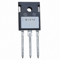
IXGH17N100AU1 IXYS, IXGH17N100AU1 Datasheet

IGBT LOW VOLT 1000V 34A TO-247AD

IXGH17N100AU1

Manufacturer Part Number
IXGH17N100AU1
Description
IGBT LOW VOLT 1000V 34A TO-247AD
Manufacturer
IXYS
Series
HiPerFAST™r
Datasheet

Specifications of IXGH17N100AU1

Voltage - Collector Emitter Breakdown (max)
1000V
Vce(on) (max) @ Vge, Ic
4V @ 15V, 17A
Current - Collector (ic) (max)
34A
Power - Max
150W
Input Type
Standard
Mounting Type
Through Hole
Package / Case
TO-247AD
Channel Type
N
Configuration
Single
Collector-emitter Voltage
1kV
Gate To Emitter Voltage (max)
±20V
Package Type
TO-247AD
Pin Count
3
Mounting
Through Hole
Operating Temperature (max)
150C
Operating Temperature Classification
Military
Vces, (v)
1000
Ic25, Tc=25°c, Igbt, (a)
34
Ic90, Tc=90°c, Igbt, (a)
17
Ic110, Tc=110°c, Igbt, (a)
-
Vce(sat), Max, Tj=25°c, Igbt, (v)
4
Tfi, Typ, Tj=25°c, Igbt, (ns)
450
Eoff, Typ, Tj=125°c, Igbt, (mj)
6
Rthjc, Max, Igbt, (°c/w)
0.83
If, Tj=110°c, Diode, (a)
17
Rthjc, Max, Diode, (ºc/w)
1.0
Package Style
TO-247
Lead Free Status / RoHS Status
Lead free / RoHS Compliant
Igbt Type
-
Lead Free Status / RoHS Status
Compliant, Lead free / RoHS Compliant

Available stocks

Company
Part Number
Manufacturer
Quantity
Price
Part Number:
IXGH17N100AU1
Manufacturer:
IXYS
Quantity:
15 500
Low V
High speed IGBT with Diode
Combi Packs
Symbol
V
V
V
V
I
I
I
SSOA
(RBSOA)
P
T
T
T
M
Weight
Maximum lead temperature for soldering
1.6 mm (0.062 in.) from case for 10 s
Symbol
BV
V
I
I
V
© 1996 IXYS All rights reserved
C25
C90
CM
CES
GES
CES
CGR
GES
GEM
C
J
JM
stg
GE(th)
CE(sat)
d
CES
CE(sat)
Test Conditions
T
T
Continuous
Transient
T
T
T
V
Clamped inductive load, L = 100 H
T
Mounting torque (M3)
Test Conditions
I
I
V
V
V
I
C
C
C
J
J
C
C
C
C
GE
CE
GE
CE
= 25 C to 150 C
= 25 C to 150 C; R
= 25 C
= 90 C
= 25 C, 1 ms
= 15 V, T
= 25 C
IGBT with Diode
= 4.5 mA, V
= 500 A, V
= 0.8 • V
= 0 V
= 0 V, V
= I
C90
, V
GE
VJ
GE
CES
= 125 C, R
= 15 V
= 20 V
GE
CE
= 0 V
= V
GE
GE
= 1 M
G
= 82
T
T
17N100U1
17N100AU1
(T
J
J
= 25 C
= 125 C
J
= 25 C, unless otherwise specified)
1000
IXGH 17 N100U1
IXGH 17 N100AU1 1000 V 34 A
min.
2.5
Characteristic Values
-55 ... +150
-55 ... +150
@ 0.8 V
Maximum Ratings
I
typ.
1.13/10 Nm/lb.in.
CM
1000
1000
= 34
150
150
300
CES
20
30
34
17
68
6
max.
500
100
5.5
3.5
4.0
8
mA
nA
W
V
V
V
V
A
A
A
A
g
V
V
V
V
C
C
C
C
A
TO-247 AD
G = Gate,
E = Emitter,
Features
Applications
Advantages
International standard package
JEDEC TO-247 AD
IGBT and anti-parallel FRED in one
package
2nd generation HDMOS
Low V
- for minimum on-state conduction
losses
MOS Gate turn-on
- drive simplicity
Fast Recovery Epitaxial Diode (FRED)
- soft recovery with low I
AC motor speed control
DC servo and robot drives
DC choppers
Uninterruptible power supplies (UPS)
Switch-mode and resonant-mode
power supplies
Saves space (two devices in one
package)
Easy to mount (isolated mounting
screw hole)
Reduces assembly time and cost
1000 V 34 A
V
G
CES
C
CE(sat)
E
C = Collector,
TAB = Collector
I
C25
TM
RM
process
91754D (3/96)
V
3.5 V
4.0 V
CE(sat)

Related parts for IXGH17N100AU1

IXGH17N100AU1 Summary of contents

Page 1

... 500 GE(th 0.8 • V CES CE CES GES CE(sat) C C90 GE © 1996 IXYS All rights reserved IXGH 17 N100U1 IXGH 17 N100AU1 1000 Maximum Ratings 1000 = 1 M 1000 0.8 V CES 150 -55 ... +150 150 -55 ... +150 1.13/10 Nm/lb.in. 6 300 Characteristic Values ( unless otherwise specified) J min. typ. ...

Page 2

... - C90 540 -di/dt = 100 thJC IXYS reserves the right to change limits, test conditions, and dimensions. IXYS MOSFETS and IGBTs are covered by one or more of the following U.S. patents: Characteristic Values ( unless otherwise specified) J min. typ. max 1500 210 40 100 = 0 CES 60 100 ...

Page 3

... Gate-Emitter Voltage Volts GE Fig. 5 Input Admittance 10V 25° 125° Volts CE © 1996 IXYS All rights reserved 150 13V 11V 125 9V 100 1 25°C J 1.3 1.2 1 34A C 1 17A C 0 8.5A 0.8 C 0.7 0.6 1.2 1.1 1.0 0.9 0.8 0 40° ...

Page 4

... D=0.1 0.1 D=0.05 D=0.02 D=0.01 Single Pulse 0.01 0.0001 0.001 IXYS reserves the right to change limits, test conditions, and dimensions. IXYS MOSFETS and IGBTs are covered by one or more of the following U.S. patents: Fig.8 Turn-Off Safe Operating Area 100 10 1 0.1 0. Duty Cycle ...

Page 5

... T - Degrees C J Fig.15 Peak Reverse Recovery Current 100° 540V 200 di /dt - A/µs F © 1996 IXYS All rights reserved Fig.12 Peak Forward Voltage 25° 2.5 3.0 3.5 Fig.14 Reverse Recovery Chargee 120 160 Fig.16 Reverse Recovery Time 0.8 max 30A F 0 ...

Page 6

... Fig.17 Diode Transient Thermal resistance junction to case 1.00 0.10 0.01 0.001 IXYS reserves the right to change limits, test conditions, and dimensions. IXYS MOSFETS and IGBTs are covered by one or more of the following U.S. patents: 0.01 Pulse Width - Seconds 4,835,592 4,881,106 4,850,072 4,931,844 ...

Related keywords