STGB10NB37LZT4 STMicroelectronics, STGB10NB37LZT4 Datasheet

IGBT N-CHAN 20A CLAMP D2PAK

STGB10NB37LZT4

Manufacturer Part Number
STGB10NB37LZT4
Description
IGBT N-CHAN 20A CLAMP D2PAK
Manufacturer
STMicroelectronics
Series
PowerMESH™r
Type
Internally Clampedr
Datasheets

Specifications of STGB10NB37LZT4

Voltage - Collector Emitter Breakdown (max)
440V
Vce(on) (max) @ Vge, Ic
1.8V @ 4.5V, 10A
Current - Collector (ic) (max)
20A
Power - Max
125W
Input Type
Logic
Mounting Type
Surface Mount
Package / Case
D²Pak, TO-263 (2 leads + tab)
Capacitance, Gate
1250 pF
Current, Collector
20 A
Package Type
D2Pak
Polarity
N-Channel
Power Dissipation
125 W
Primary Type
Si
Resistance, Thermal, Junction To Case
1.2 °C/W
Voltage, Collector To Emitter Shorted
Clamped
Voltage, Collector To Emitter, Saturation
1.2 V
Lead Free Status / RoHS Status
Lead free / RoHS Compliant
Igbt Type
-
Lead Free Status / Rohs Status
RoHS Compliant part Electrostatic Device
Other names
497-4106-2

Available stocks

Company
Part Number
Manufacturer
Quantity
Price
Part Number:
STGB10NB37LZT4
Manufacturer:
DIODES
Quantity:
15 000
Part Number:
STGB10NB37LZT4
Manufacturer:
ST
0
Company:
Part Number:
STGB10NB37LZT4
Quantity:
9 000
Part Number:
STGB10NB37LZT4G
Manufacturer:
ST
0
DESCRIPTION
Using the latest high voltage technology based on a
patented strip layout, STMicroelectronics has
designed an advanced family of IGBTs, the
PowerMESH
performances. The built in collector-gate zener
exhibits a very precise active clamping while the
gate-emitter zener supplies an ESD protection.
APPLICATIONS
ABSOLUTE MAXIMUM RATINGS
STGB10NB37LZ
POLYSILICON GATE VOLTAGE DRIVEN
LOW THRESHOLD VOLTAGE
LOW ON-VOLTAGE DROP
LOW GATE CHARGE
HIGH CURRENT CAPABILITY
HIGH VOLTAGE CLAMPING FEATURE
AUTOMOTIVE IGNITION
Symbol
V
V
P
V
E
T
I
CES
ECR
CM
I
TOT
T
stg
GE
SD
C
TYPE
j
Collector-Emitter Voltage (V
Reverse Battery Protection
Gate-Emitter Voltage
Collector Current (continuos) at T
Collector Current (pulse width < 100 s)
Total Dissipation at T
Derating Factor
ESD (Human Body Model)
Storage Temperature
Max. Operating Junction Temperature
IGBTs, with outstanding
CLAMPED
V
CES
INTERNALLY CLAMPED PowerMesh™ IGBT
V
< 1.8 V
C
CE(sat)
Parameter
= 25°C
GS
= 0)
N-CHANNEL CLAMPED 20A - D2PAK
C
20 A
= 100°C
I
C
INTERNAL SCHEMATIC DIAGRAM
STGB10NB37LZ
CLAMPED
CLAMPED
–65 to 175
D2PAK
Value
0.83
125
175
18
20
60
4
1
3
W/°C
Unit
KV
°C
°C
W
V
V
V
A
A
1/10

Related parts for STGB10NB37LZT4

STGB10NB37LZT4 Summary of contents

Page 1

... LOW ON-VOLTAGE DROP LOW GATE CHARGE HIGH CURRENT CAPABILITY HIGH VOLTAGE CLAMPING FEATURE DESCRIPTION Using the latest high voltage technology based on a patented strip layout, STMicroelectronics has designed an advanced family of IGBTs, the ™ PowerMESH IGBTs, with outstanding performances. The built in collector-gate zener exhibits a very precise active clamping while the gate-emitter zener supplies an ESD protection ...

Page 2

STGB10NB37LZ THERMAL DATA Rthj-case Thermal Resistance Junction-case Max Rthj-amb Thermal Resistance Junction-ambient Max Rthc-sink Thermal Resistance Case-sink Typ ELECTRICAL CHARACTERISTICS (TCASE = 25 °C UNLESS OTHERWISE SPECIFIED) OFF Symbol Parameter BV Clamped Voltage (CES) BV Emitter Collector Break-down (ECR) Voltage ...

Page 3

FUNCTIONAL CHARACTERISTICS Symbol Parameter I Latching Current L U.I.S. Unclamped Inductive Switching Current SWITCHING ON Symbol Parameter t Turn-on Delay Time d(on) t Rise Time r (di/dt) Turn-on Current Slope on Turn-on Switching Losses Eon SWITCHING OFF Symbol Parameter t ...

Page 4

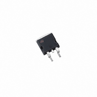
STGB10NB37LZ DIM. MIN. A 4.4 A1 2.49 A2 0.03 B 0.7 B2 1.14 C 0.45 C2 1. 1.27 L3 1 0º 8/ PAK ...

Page 5

D PAK FOOTPRINT TAPE AND REEL SHIPMENT (suffix ”T4”)* TAPE MECHANICAL DATA mm inch DIM. MIN. MAX. MIN. A0 10.5 10.7 0.413 0.421 B0 15.7 15.9 0.618 0.626 D 1.5 1.6 0.059 0.063 D1 1.59 1.61 0.062 0.063 E ...

Related keywords