PMEG2020AEA,115 NXP Semiconductors, PMEG2020AEA,115 Datasheet - Page 3
PMEG2020AEA,115
Manufacturer Part Number
PMEG2020AEA,115
Description
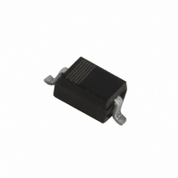
SCHOTTKY RECT 20V 2A SOD323
Manufacturer
NXP Semiconductors
Datasheet
1.PMEG2020AEA115.pdf
(7 pages)
Specifications of PMEG2020AEA,115
Package / Case
SC-76, SOD-323, UMD2
Mounting Type
Surface Mount
Speed
Fast Recovery =< 500ns, > 200mA (Io)
Current - Reverse Leakage @ Vr
200µA @ 20V
Voltage - Forward (vf) (max) @ If
525mV @ 2A
Voltage - Dc Reverse (vr) (max)
20V
Capacitance @ Vr, F
70pF @ 5V, 1MHz
Current - Average Rectified (io)
2A (DC)
Product
Schottky Diodes
Peak Reverse Voltage
20 V
Forward Continuous Current
2 A
Max Surge Current
9 A
Configuration
Single
Forward Voltage Drop
0.525 V
Maximum Reverse Leakage Current
200 uA
Operating Temperature Range
+ 150 C
Mounting Style
SMD/SMT
Lead Free Status / RoHS Status
Lead free / RoHS Compliant
Reverse Recovery Time (trr)
-
Lead Free Status / Rohs Status
Lead free / RoHS Compliant
Other names
934057933115::PMEG2020AEA T/R::PMEG2020AEA T/R
Available stocks
Company
Part Number
Manufacturer
Quantity
Price

Part Number:
PMEG2020AEA,115
Manufacturer:
NXP/恩智浦
Quantity:
20 000


NXP Semiconductors
LIMITING VALUES
In accordance with the Absolute Maximum Rating System (IEC 60134)
THERMAL CHARACTERISTICS
Notes
1. Refer to SOD323 (SC-76) standard mounting conditions.
2. For Schottky barrier diodes thermal runaway has to be considered, as in some applications, the reverse power losses
3. Device mounted on a on an FR4 printed-circuit board with copper clad 10 x 10 mm.
4. Soldering point of cathode tab.
ELECTRICAL CHARACTERISTICS
T
Note
1. Pulse test: t
2004 Feb 26
V
I
I
I
T
T
T
R
R
R
V
I
C
SYMBOL
F
FRM
FSM
j
R
SYMBOL
SYMBOL
stg
j
amb
R
= 25 °C unless otherwise specified.
F
20 V, 2 A very low V
barrier rectifier in SOD323 (SC-76) package
th(j-a)
th(j-a)
th(j-s)
d
P
I
F
R
(AV) rating will be available on request.
are a significant part of the total power losses. Nomograms for determination of the reverse power losses P
thermal resistance from junction to ambient
thermal resistance from junction to ambient
thermal resistance from junction to solder point note 4
continuous reverse voltage
continuous forward current
repetitive peak forward current
non-repetitive peak forward current
storage temperature
junction temperature
operating ambient temperature
forward voltage
reverse current
diode capacitance
p
≤ 300 μs; δ ≤ 0.02.
PARAMETER
PARAMETER
PARAMETER
F
MEGA Schottky
see Fig.2; note 1
V
V
V
V
R
R
R
R
I
I
I
I
T
t
t = 8 ms square wave
F
F
F
F
p
= 5 V; see Fig.3
= 10 V
= 20 V
sp
= 5 V; f = 1 MHz; see Fig.4
= 0.01 A
= 0.1 A
= 1 A
= 2 A
≤ 1 ms; δ ≤ 0.25
≤ 55 °C
3
CONDITIONS
notes 1 and 2
notes 2 and 3
CONDITIONS
CONDITIONS
−
−
−
−
−65
−
−65
200
265
380
450
15
20
50
55
MIN.
TYP.
VALUE
PMEG2020AEA
450
210
90
20
2
7
9
+150
150
+150
220
290
430
525
50
80
200
70
Product data sheet
MAX.
MAX.
UNIT
K/W
K/W
K/W
V
A
A
A
°C
°C
°C
mV
mV
mV
mV
μA
μA
μA
pF
UNIT
UNIT
R
and
Related parts for PMEG2020AEA,115
Image
Part Number
Description
Manufacturer
Datasheet
Request
R

Part Number:
Description:
NXP Semiconductors designed the LPC2420/2460 microcontroller around a 16-bit/32-bitARM7TDMI-S CPU core with real-time debug interfaces that include both JTAG andembedded trace
Manufacturer:
NXP Semiconductors
Datasheet:

Part Number:
Description:
NXP Semiconductors designed the LPC2458 microcontroller around a 16-bit/32-bitARM7TDMI-S CPU core with real-time debug interfaces that include both JTAG andembedded trace
Manufacturer:
NXP Semiconductors
Datasheet:
Part Number:
Description:
NXP Semiconductors designed the LPC2468 microcontroller around a 16-bit/32-bitARM7TDMI-S CPU core with real-time debug interfaces that include both JTAG andembedded trace
Manufacturer:
NXP Semiconductors
Datasheet:
Part Number:
Description:
NXP Semiconductors designed the LPC2470 microcontroller, powered by theARM7TDMI-S core, to be a highly integrated microcontroller for a wide range ofapplications that require advanced communications and high quality graphic displays
Manufacturer:
NXP Semiconductors
Datasheet:
Part Number:
Description:
NXP Semiconductors designed the LPC2478 microcontroller, powered by theARM7TDMI-S core, to be a highly integrated microcontroller for a wide range ofapplications that require advanced communications and high quality graphic displays
Manufacturer:
NXP Semiconductors
Datasheet:
Part Number:
Description:
The Philips Semiconductors XA (eXtended Architecture) family of 16-bit single-chip microcontrollers is powerful enough to easily handle the requirements of high performance embedded applications, yet inexpensive enough to compete in the market for hi
Manufacturer:
NXP Semiconductors
Datasheet:
Part Number:
Description:
The XA-S3 device is a member of Philips Semiconductors? XA(eXtended Architecture) family of high performance 16-bitsingle-chip microcontrollers
Manufacturer:
NXP Semiconductors
Datasheet:

Part Number:
Description:
The NXP BlueStreak LH75401/LH75411 family consists of two low-cost 16/32-bit System-on-Chip (SoC) devices
Manufacturer:
NXP Semiconductors
Datasheet:
Part Number:
Description:
The NXP LPC3130/3131 combine an 180 MHz ARM926EJ-S CPU core, high-speed USB2
Manufacturer:
NXP Semiconductors
Datasheet:
Part Number:
Description:
The NXP LPC3141 combine a 270 MHz ARM926EJ-S CPU core, High-speed USB 2
Manufacturer:
NXP Semiconductors
Part Number:
Description:
The NXP LPC3143 combine a 270 MHz ARM926EJ-S CPU core, High-speed USB 2
Manufacturer:
NXP Semiconductors

Part Number:
Description:
The NXP LPC3152 combines an 180 MHz ARM926EJ-S CPU core, High-speed USB 2
Manufacturer:
NXP Semiconductors
Part Number:
Description:
The NXP LPC3154 combines an 180 MHz ARM926EJ-S CPU core, High-speed USB 2
Manufacturer:
NXP Semiconductors

Part Number:
Description:
Standard level N-channel enhancement mode Field-Effect Transistor (FET) in a plastic package using NXP High-Performance Automotive (HPA) TrenchMOS technology
Manufacturer:
NXP Semiconductors
Datasheet: