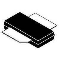
MRF8S9102NR3 Freescale Semiconductor, MRF8S9102NR3 Datasheet

MRF8S9102NR3
Specifications of MRF8S9102NR3
Available stocks
Related parts for MRF8S9102NR3
MRF8S9102NR3 Summary of contents
Page 1
... Designed for out = 28 Volts Output PAR ACPR η D (%) (dB) (dBc) 6.4 --34.7 6.2 --35.1 6.0 --35.7 Document Number: MRF8S9102N Rev. 0, 2/2011 MRF8S9102NR3 865- -960 MHz AVG SINGLE W- -CDMA LATERAL N- -CHANNEL RF POWER MOSFET CASE 2021- -03, STYLE 1 OM- -780- -2 PLASTIC MRF8S9102NR3 1 ...
Page 2
... Refer to AN1955, Thermal Measurement Methodology of RF Power Amplifiers http://www.freescale.com/rf. Select Documentation/Application Notes -- AN1955 Parameter measured on Freescale Test Fixture, due to resistive divider network on the board. Refer to Test Circuit GG GS(Q) schematic. MRF8S9102NR3 2 = 750 mA, 880 MHz DQ = 750 mA, 880 MHz DQ Rating 3 = 25°C unless otherwise noted) ...
Page 3
... Vdc 750 mA Avg out Output PAR ACPR η D (%) (dB) (dBc) 35.4 6.4 --34.7 35.5 6.2 --35.1 35.6 6.0 --35.7 MRF8S9102NR3 Unit dBc dB IRL (dB) --14 --22 --17 W MHz MHz dB dB/°C dB/°C IRL (dB) --15 --23 --19 3 ...
Page 4
... MRF8S9102N Rev. 0 Figure 1. MRF8S9102NR3 Test Circuit Component Layout Table 6. MRF8S9102NR3 Test Circuit Component Designations and Values Part C1, C2 220 μ Electrolytic Capacitors C3, C4, C5, C6 μ Chip Capacitors C8, C14, C15 3.0 pF Chip Capacitors C9, C12, C13, C16 47 pF Chip Capacitors C10 4.3 pF Chip Capacitor C11 4 ...
Page 5
... MHz, Single--Carrier OUTPUT POWER (WATTS) out Figure 4. Output Peak- -to- -Average Ratio Compression (PARC) versus Output Power --36 --0.5 0 --36.5 --0.8 --5 --37 --1.1 --10 PARC --37.5 --1.4 --15 --38 --1.7 --20 --38.5 --2 --25 960 980 100 --20 60 η --25 ACPR -- --40 20 --45 10 PARC -- MRF8S9102NR3 5 ...
Page 6
... Channel Bandwidth @ ±5 MHz Offset. 0.001 Input Signal PAR = 7 0.01% Probability on CCDF 0.0001 PEAK--TO--AVERAGE (dB) Figure 7. CCDF W- -CDMA IQ Magnitude Clipping, Single- -Carrier Test Signal MRF8S9102NR3 6 TYPICAL CHARACTERISTICS 920 MHz G 940 MHz ps 960 MHz = 28 Vdc 750 mA, Single--Carrier DD DQ 960 MHz 940 MHz ...
Page 7
... Z = Test circuit impedance as measured from source gate to ground Test circuit impedance as measured from load drain to ground. Device Input Matching Under Test Network Z Z source load Output Matching Network MRF8S9102NR3 7 ...
Page 8
... ALTERNATIVE PEAK TUNE LOAD PULL CHARACTERISTICS NOTE: Load Pull Test Fixture Tuned for Peak P1dB Output Power @ 28 V MRF8S9102NR3 Vdc 750 mA, Pulsed CW, 10 μsec(on), 10% Duty Cycle DD DQ Ideal 920 MHz 920 MHz 960 MHz 940 MHz INPUT POWER (dBm) in P1dB f Watts ...
Page 9
... C17 MRF8S9102N Rev. 0 Figure 11. MRF8S9102NR3 Test Circuit Component Layout — 865- -895 MHz Table 7. MRF8S9102NR3 Test Circuit Component Designations and Values — 865- -895 MHz Part C1, C2 220 μ Electrolytic Capacitors C3, C4, C5, C6 μ Chip Capacitors C8 2.7 pF Chip Capacitor C9, C12, C13, C16 ...
Page 10
... W--CDMA, 3.84 MHz Channel Bandwidth Input Signal PAR = 7 0.01% Probability on CCDF Figure 13. Single- -Carrier W- -CDMA Power Gain, Drain 700 MRF8S9102NR3 Vdc (Avg.), I = 750 mA DD out DQ 3.84 MHz Channel Bandwidth Input Signal PAR = 7 0.01% Probability on CCDF PARC ACPR IRL 840 860 ...
Page 11
... Z = Test circuit impedance as measured from source gate to ground Test circuit impedance as measured from load drain to ground. Device Input Matching Under Test Network Z Z source load Output Matching Network MRF8S9102NR3 11 ...
Page 12
... MRF8S9102NR3 12 PACKAGE DIMENSIONS RF Device Data Freescale Semiconductor ...
Page 13
... RF Device Data Freescale Semiconductor MRF8S9102NR3 13 ...
Page 14
... MRF8S9102NR3 14 RF Device Data Freescale Semiconductor ...
Page 15
... For Software Part Number search at http://www.freescale.com, and select the “Part Number” link the Software & Tools tab on the part’s Product Summary page to download the respective tool. The following table summarizes revisions to this document. Revision Date 0 Feb. 2011 • Initial Release of Data Sheet RF Device Data Freescale Semiconductor REVISION HISTORY Description MRF8S9102NR3 15 ...
Page 16
... For Literature Requests Only: Freescale Semiconductor Literature Distribution Center 1--800--441--2447 or +1--303--675--2140 Fax: +1--303--675--2150 LDCForFreescaleSemiconductor@hibbertgroup.com MRF8S9102NR3 Document Number: MRF8S9102N Rev. 0, 2/2011 16 Information in this document is provided solely to enable system and software implementers to use Freescale Semiconductor products. There are no express or implied copyright licenses granted hereunder to design or fabricate any integrated circuits or integrated circuits based on the information in this document ...


