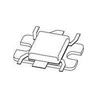
BLF6G27L-50BN,112 NXP Semiconductors, BLF6G27L-50BN,112 Datasheet - Page 9

BLF6G27L-50BN,112
Manufacturer Part Number
BLF6G27L-50BN,112
Description
RF MOSFET Power Single 65V 0.25Ohms
Manufacturer
NXP Semiconductors
Datasheet
1.BLF6G27L-50BN112.pdf
(16 pages)
Specifications of BLF6G27L-50BN,112
Mounting Style
SMD/SMT
Resistance Drain-source Rds (on)
0.25 Ohms
Transistor Polarity
N-Channel
Configuration
Single
Drain-source Breakdown Voltage
65 V
Package / Case
SOT-1112A
Lead Free Status / RoHS Status
Lead free / RoHS Compliant
NXP Semiconductors
BLF6G27L-50BN_6G27LS-50BN
Product data sheet
Fig 13. Single carrier W-CDMA peak-to-average power
PAR
(1) f = 2500 MHz
(2) f = 2600 MHz
(3) f = 2700 MHz
9.0
7.5
6.0
4.5
3.0
1.5
0
V
ratio as a function of load power;
typical values
DS
= 28 V; I
7.5 Single carrier W-CDMA
5
Dq
(1)
(2)
(3)
= 430 mA.
All testing performed in Class-AB production test circuit; test signal 3GPP; test model 1;
64 DPCH; PAR = 7.2 dB at 0.01 % probability on CCDF per carrier; f = 2700 MHz;
T
10
case
= 25 °C; unless otherwise specified.
15
20
All information provided in this document is subject to legal disclaimers.
001aan493
P
L
(W)
25
Rev. 2 — 7 April 2011
Fig 14. Single carrier W-CDMA peak output power as a
P
(W)
L(M)
(1) f = 2500 MHz
(2) f = 2600 MHz
(3) f = 2700 MHz
100
80
60
40
20
0
0
V
function of load power; typical values
DS
= 28 V; I
BLF6G27L(S)-50BN
5
Dq
= 430 mA.
10
Power LDMOS transistor
15
© NXP B.V. 2011. All rights reserved.
20
001aan494
(1)
(2)
(3)
P
L
(W)
25
9 of 16


